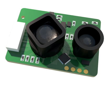
In modern industrial manufacturing, achieving precise flatness measurement is critical for ensuring product quality, assembly accuracy, and operational efficiency. Laser sensors have emerged as a premier solution for non-contact, high-speed flatness inspection across various sectors, including automotive, aerospace, electronics, and heavy machinery. Unlike traditional mechanical methods that involve physical contact and potential surface damage, laser sensors utilize focused light beams to capture detailed topographical data without touching the target surface.
The fundamental principle behind laser-based flatness measurement involves triangulation or time-of-flight techniques. In triangulation-based sensors, a laser diode projects a visible or infrared spot onto the target surface. The reflected light is captured by a high-resolution CMOS or CCD detector at a known angle. Any variation in surface height causes a shift in the position of the reflected spot on the detector. By calculating this displacement using trigonometric algorithms, the sensor determines the exact distance to each measured point. For larger surfaces, multiple sensors or scanning laser systems are deployed to create a comprehensive 3D profile. Time-of-flight sensors, on the other hand, measure the phase shift or flight time of modulated laser pulses to compute distance, suitable for longer ranges but typically with slightly lower resolution compared to triangulation methods.
Key advantages of laser sensors in flatness measurement include sub-micron accuracy, rapid data acquisition rates exceeding 10 kHz, and immunity to environmental factors like electromagnetic interference when properly shielded. They can detect minute deviations, warping, or waviness that might be invisible to the human eye or conventional tools. In practice, these sensors are integrated into automated inspection stations, robotic arms, or CNC machine tools. For instance, in semiconductor wafer production, laser sensors verify the planarity of substrates to prevent lithography defects. In metal stamping, they ensure pressed sheets meet flatness tolerances before assembly.
Implementation requires careful consideration of surface properties. Highly reflective or transparent materials may necessitate sensors with adjustable power or specialized filters to avoid signal saturation or loss. Ambient lighting conditions and vibration also influence measurement stability, often addressed through hardware enclosures and software filtering. Calibration against master reference surfaces is essential to maintain traceability to international standards like ISO 1101.
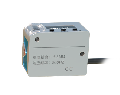
Data processing plays a pivotal role. Advanced software algorithms analyze point clouds to calculate flatness parameters such as Peak-to-Valley (PV) deviation, root mean square (RMS) roughness, and overall flatness error relative to a defined datum plane. Real-time feedback enables immediate corrective actions in production lines, reducing scrap and rework. Emerging trends include integration with Industry 4.0 platforms, where laser measurement data feeds into digital twins for predictive maintenance and process optimization.
Despite their robustness, laser sensors are not a universal panacea. They may struggle with extremely dark, absorptive surfaces that scatter insufficient light, requiring alternative solutions like confocal chromatic sensors. Regular maintenance, including lens cleaning and periodic recalibration, ensures long-term accuracy.
In summary, laser sensors provide a reliable, efficient, and scalable method for flatness measurement, driving quality assurance in precision manufacturing. Their ability to deliver non-contact, high-resolution 3D data makes them indispensable for applications demanding stringent geometrical tolerances. As sensor technology advances with improvements in miniaturization, cost-effectiveness, and smart connectivity, their adoption is set to expand further, reinforcing their role as a cornerstone of modern metrology.