For electrical engineers and technical professionals, mastering the assembly and interpretation of laser sensor diagrams is crucial for ensuring precision, reliability, and optimal performance in various industrial applications. This guide delves into the essential components, standard practices, and common pitfalls associated with laser sensor assembly, providing a detailed walkthrough to enhance your technical proficiency.
Laser sensors operate by emitting a focused light beam to detect objects, measure distances, or monitor processes with high accuracy. The assembly diagram serves as a foundational blueprint, detailing the integration of optical, electronic, and mechanical parts. Key components typically include the laser diode, which generates the coherent light; lenses or collimators to focus the beam; photodetectors (such as photodiodes or CCD arrays) to capture reflected signals; signal processing circuits for data interpretation; and housing units that ensure environmental protection and alignment stability. Each element must be meticulously aligned according to the diagram specifications to prevent signal degradation or operational failures.
When interpreting an assembly diagram, start by reviewing the schematic symbols and annotations. Standard symbols denote components like resistors, capacitors, and integrated circuits, while optical paths are often represented with dashed lines. Pay close attention to tolerance levels, indicated by +/- values, as even minor deviations can impact sensor accuracy. For instance, misalignment of the laser diode by a few micrometers might lead to beam divergence, reducing detection range. Diagrams also specify wiring connections—typically color-coded for power (red/black), ground (green/yellow), and output signals (blue/white)—ensuring proper integration with control systems like PLCs or microcontrollers.
Assembly begins with preparing a clean, static-free workspace to avoid contamination of sensitive optical surfaces. Mount the laser diode onto its heat sink using thermal conductive adhesive, as overheating can shorten component lifespan. Next, secure the focusing lens in its holder, adjusting the set screws per the diagram’s angular measurements to achieve the desired beam profile. Connect the photodetector to the processing board via soldered joints or connectors, verifying continuity with a multimeter. Throughout the process, refer to the diagram’s cross-sectional views to confirm spatial relationships between parts, especially in compact designs where space constraints are critical.
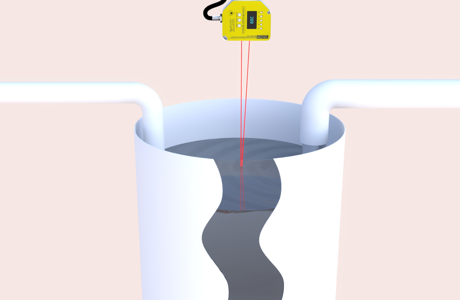
Testing and calibration are integral steps post-assembly. Use an oscilloscope to monitor the output waveform, comparing it against the diagram’s expected signal parameters. Adjust potentiometers or software settings if the response time or sensitivity deviates from specifications. For distance-measuring sensors, validate accuracy with calibrated targets at known intervals, noting any discrepancies in the diagram’s performance curves. Common issues, such as electrical noise interference or lens fogging, can often be traced to diagram oversights—like inadequate shielding or improper sealing—highlighting the importance of thorough review before assembly.
In industrial settings, laser sensor assemblies must comply with safety standards (e.g., IEC 60825 for radiation limits) and environmental ratings (IP67 for dust/water resistance). Diagrams should include notes on compliant materials and installation guidelines, such as using lock washers on mounting bolts to prevent vibration-induced loosening. Advanced diagrams may incorporate 3D exploded views or digital twins for virtual validation, streamlining troubleshooting and maintenance. By adhering to these diagrams, engineers can optimize sensor longevity and reduce downtime in applications from automated manufacturing to robotics.
Ultimately, a well-crafted laser sensor assembly diagram is more than a technical drawing—it’s a roadmap to innovation. As sensor technology evolves with trends like miniaturization and IoT integration, diagrams will continue to bridge design intent with practical execution. Regular training on diagram interpretation, coupled with hands-on practice, empowers engineers to tackle complex projects confidently, ensuring that every assembled sensor meets the rigorous demands of modern industry.