Proximity sensors are fundamental components in modern industrial automation, robotics, and safety systems. Their primary function is to detect the presence or absence of an object within a specified range without physical contact. While much attention is given to sensing technologies like inductive, capacitive, ultrasonic, and photoelectric, the output stage—the electrical interface that communicates the detection event to the control system—is equally critical. This article delves into the output schematic principles of common proximity sensors, explaining the circuitry that translates a sensing event into a usable electrical signal.
The core of any proximity sensor is the oscillator and detection circuit specific to its technology. For instance, an inductive sensor uses a coil in an oscillator circuit; when a metallic object enters its field, it dampens the oscillations. This change is detected, but it must be converted into a clean, standardized output signal. This is where the output stage comes into play. The most prevalent output types are Digital Outputs: NPN (Sinking), PNP (Sourcing), and Push-Pull, along with Analog Outputs (typically 4-20 mA or 0-10V).
Let's examine the schematic principles for a standard DC 3-wire sensor with a digital transistor output. Such a sensor has three connections: V+ (Brown wire, typically +12V to +24V DC), V- (Blue wire, 0V/GND), and the Output wire (Black for NPN, Black or sometimes White for PNP).
NPN (Sinking) Output Schematic:
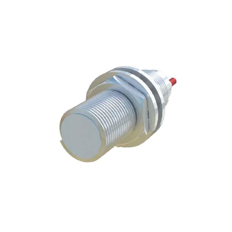
In an NPN output configuration, the output transistor is an NPN bipolar junction transistor (BJT) or an N-channel MOSFET. In the schematic, the load (e.g., a PLC input, relay coil) is connected between the sensor's output terminal and the positive supply voltage (V+). The sensor's output terminal is effectively the collector (for BJT) or drain (for MOSFET) of the transistor. The emitter/source is connected internally to the negative supply (V-). When the sensor detects an object, the transistor switches ON, creating a low-resistance path from the output terminal to V-. This "sinks" current from the load down to ground, activating it. The output voltage, when active, drops to a low saturation voltage (e.g.,<1V). When inactive, the transistor is OFF, and the output is in a high-impedance state. The load sees an open circuit, and its voltage can be pulled up to V+ by an external or internal pull-up resistor if present.
PNP (Sourcing) Output Schematic:
The PNP output uses a PNP BJT or a P-channel MOSFET. Here, the load is connected between the sensor's output terminal and the negative supply (V-). The output terminal is the emitter (BJT) or source (MOSFET). The collector/drain is connected internally to V+. Upon detection, the transistor switches ON, "sourcing" current from V+ through the transistor and the load to V-. The output voltage, when active, rises to near the supply voltage (V+ minus a small saturation voltage). When inactive, the transistor is OFF, and the output is again high-impedance, potentially pulled low by an external resistor.
Push-Pull (Complementary) Output Schematic:
This configuration combines both NPN and PNP transistors (or N and P-channel MOSFETs) in a complementary pair. It can both source and sink current actively. The schematic shows the two transistors connected in series between V+ and V-, with the output taken from their junction. Control logic ensures they are never on simultaneously (to prevent a short circuit). When active, one transistor turns on to drive the output high or low with a low impedance. This makes it versatile for interfacing with various loads without worrying about external pull-up/down resistors.
Analog Output Schematic:
For analog sensors, the output stage is more complex. After signal conditioning and amplification of the sensed parameter (e.g., distance), the signal drives a voltage-to-current converter circuit for a 4-20 mA output or a linear amplifier for a 0-10V output. A classic 4-20 mA transmitter schematic often uses an operational amplifier in a feedback configuration with a transistor to regulate the loop current precisely, independent of supply voltage variations within limits. The 4 mA "live zero" ensures loop integrity detection.
Key Schematic Components and Protection:
Beyond the core switching element, a robust output schematic includes several protective and functional components:
1. Reverse Polarity Protection: A series diode or a bridge rectifier protects the internal circuitry if power wires are connected incorrectly.
2. Voltage Regulation/Stabilization: Zener diodes or integrated regulators provide stable voltage for the sensor's oscillator and