In modern industrial automation and precision measurement systems, laser sensors have become indispensable tools for non-contact detection, distance measurement, and profile scanning. The accuracy and reliability of these sensors heavily depend on the quality of the Analog-to-Digital Conversion (ADC) process that translates the sensor's analog output into digital data for processing. This article delves into the critical aspects of laser sensor AD sampling, exploring principles, challenges, and best practices for engineers.
The core function of a laser sensor, such as a time-of-flight (ToF) or triangulation-based sensor, is to emit a laser beam and measure the properties of the reflected light. This reflection generates a minute analog signal—typically a voltage or current—whose characteristics (amplitude, phase, time delay) correlate directly with the measured parameter (e.g., distance, presence, thickness). This analog signal is inherently continuous and susceptible to noise. The ADC's role is to sample this signal at discrete intervals and quantize it into binary numbers, creating a digital representation that microcontrollers or processors can interpret.
Selecting an appropriate ADC is paramount. Key specifications include resolution, sampling rate, and signal-to-noise ratio (SNR). Resolution, measured in bits (e.g., 12-bit, 16-bit), determines the smallest change in the analog signal the ADC can detect. For high-precision laser measurement where micron-level accuracy is required, a 16-bit or higher ADC is often necessary. The sampling rate must be sufficiently high to capture rapid changes in the measured target, adhering to the Nyquist theorem to avoid aliasing. For dynamic measurements, sampling rates in the kilohertz or megahertz range may be needed.
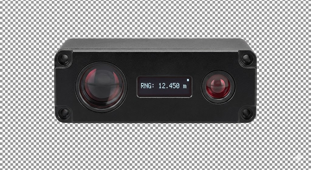
However, the path from the laser sensor's photodiode or receiver to the ADC input is fraught with potential signal degradation. Environmental electrical noise, thermal noise from components, and crosstalk can corrupt the delicate analog signal. Therefore, a well-designed signal conditioning circuit preceding the ADC is non-negotiable. This typically involves:
1. A transimpedance amplifier (TIA) to convert the photodiode's current signal into a stable voltage.
2. Passive or active filtering (low-pass, band-pass) to eliminate out-of-band noise and interference, especially from ambient light or power line harmonics (50/60 Hz).

3. Proper shielding and grounding of cables and PCB layouts to minimize electromagnetic interference (EMI).
4. Sometimes, a programmable gain amplifier (PGA) to scale the signal optimally to match the ADC's input voltage range, maximizing dynamic range.
The architecture of the ADC itself also influences performance. Successive Approximation Register (SAR) ADCs offer a good balance of speed and resolution for many laser sensing applications. Delta-Sigma (ΔΣ) ADCs provide very high resolution and excellent noise rejection at lower speeds, ideal for high-accuracy static or slow-moving measurements. Integrating the ADC into the system requires careful management of reference voltages, which must be stable and low-noise, as any fluctuation directly impacts measurement accuracy.
Firmware and software play a crucial role in extracting meaningful data. Oversampling and averaging techniques can effectively increase resolution and reduce random noise. Implementing digital filters (e.g., moving average, finite impulse response filters) in the microcontroller can further smooth the data. For ToF sensors, sophisticated algorithms are used to calculate distance from the sampled phase or time data. Calibration is essential; engineers must develop procedures to compensate for sensor offset, gain errors, and non-linearities across the operating temperature range, often storing calibration coefficients in non-volatile memory.
In practical applications, such as robotic guidance, thickness gauging, or vibration analysis, the entire signal chain—from the laser emitter optics to the digital data output—must be treated as a single system. Regular validation against traceable standards ensures long-term precision. Furthermore, understanding the target surface properties (color, reflectivity, texture) is vital, as they affect signal strength and may require adaptive sampling strategies.
In conclusion, achieving high-fidelity digital data from a laser sensor is a multidisciplinary challenge spanning optics, analog circuit design, digital conversion, and software algorithm development. By meticulously addressing each stage of the AD sampling process—through thoughtful component selection, robust signal conditioning, and intelligent data processing—engineers can unlock the full potential of laser sensing technology, enabling breakthroughs in manufacturing quality control, autonomous systems, and scientific research. The pursuit of higher resolution, faster sampling, and greater noise immunity continues to drive innovation in this critical field.