In the realm of industrial automation and control systems, proximity switch sensors are indispensable components for non-contact detection of metallic or non-metallic objects. However, their performance can be severely compromised by electromagnetic interference (EMI), radio frequency interference (RFI), and other environmental noise sources. This article delves into the critical role of anti-interference features in proximity sensors, supported by a detailed visual guide to their design, installation, and application through technical images. Understanding the visual characteristics of these sensors is paramount for engineers and technicians aiming to ensure reliable operation in harsh industrial environments.
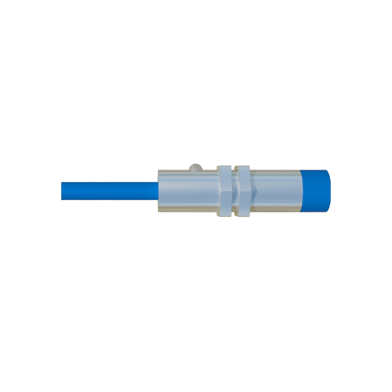
A primary visual indicator of an anti-interference proximity sensor is its robust housing design. High-quality images often reveal sensors encased in stainless steel or nickel-plated brass bodies, providing not just physical durability but also inherent shielding against external electromagnetic fields. The housing is typically sealed to IP67 or IP69K standards, evident from the visible gaskets and tight seams, which prevent ingress of dust and moisture—common culprits of signal disruption. Close-up photographs frequently highlight the sensor face, which may be made of materials like PBT or PTFE, offering resistance to chemical exposure and contributing to stable sensing performance by minimizing false triggers from surrounding contaminants.
The internal construction, as illustrated in cross-sectional diagrams and exploded-view images, is where advanced anti-interference technology becomes visually apparent. Key components include shielded cables with thick, braided copper sheathing, clearly visible in cutaway photos, which divert interference away from the sensitive oscillator and amplifier circuits. Circuit board images often show the use of surface-mount devices (SMDs) arranged to minimize loop areas, alongside ferrite beads and capacitors placed near signal lines to filter out high-frequency noise. Some sensors incorporate dedicated ASICs (Application-Specific Integrated Circuits), visible as compact black chips on the PCB, which are programmed with algorithms to distinguish between genuine target signals and environmental noise, enhancing noise immunity.
Wiring and connection diagrams are crucial visual aids. These schematics typically depict the correct grounding practices, such as the use of a separate ground wire connected directly to the sensor's metal housing or a designated earth point, which is vital for draining interference. Images of installation setups emphasize maintaining a minimum distance between sensor cables and high-voltage power lines, often recommending separation by several centimeters or using shielded conduit, visually represented in layout drawings. Diagrams also illustrate the importance of avoiding parallel runs with motor cables or frequency inverters, instead showing crossed cable routing at 90-degree angles to reduce inductive coupling.
The application of anti-interference proximity sensors is best understood through real-world imagery. In automotive manufacturing plants, photos show sensors mounted on robotic arms, their compact and shielded designs enabling precise detection amidst welding sparks and strong electromagnetic fields from large motors. In food processing facilities, images depict sensors with hygienic, smooth surfaces and high IP ratings, operating reliably despite frequent washdowns and steam, which could otherwise cause electrical noise. Another compelling visual example is from CNC machining centers, where sensors are installed near spindle drives and servo motors; detailed photos highlight their immunity to the intense EMI generated by these high-speed components, ensuring accurate tool positioning and part detection without erroneous signals.
Selecting the right sensor involves interpreting specification sheets and visual catalogs. Key images to scrutinize include graphs depicting noise immunity levels, usually measured in volts per meter (V/m) for RFI or millivolts for conducted interference. Comparative photos between standard and anti-interference models may show additional filtering components or enhanced shielding. It is also advisable to review test setup images from manufacturers, demonstrating compliance with standards like IEC 60947-5-2, which validate the sensor's performance under simulated interference conditions. These visuals provide concrete evidence of the sensor's capability to maintain a stable switching state despite surrounding electrical noise.
In conclusion, anti-interference proximity switch sensors are engineered with specific visual and structural features to combat industrial noise. From their fortified housings and internal shielding to proper installation geometries, each element plays a role in ensuring signal integrity. By carefully analyzing technical images—including housing details, internal layouts, wiring diagrams, and application photos—professionals can make informed decisions to enhance system reliability. As industries evolve towards greater connectivity and automation, the demand for visually identifiable, interference-immune sensing solutions will only intensify, making this visual knowledge essential for optimal system design and maintenance.