In the realm of industrial automation and machine safety, proximity sensors stand as critical components, enabling non-contact detection of metallic and non-metallic objects. Their reliability is paramount, and this reliability is forged within a meticulously controlled manufacturing process. This article delves into the comprehensive production workflow of a standard inductive proximity sensor, outlining the key stages from raw material to final testing and packaging.
The journey begins with the procurement and inspection of high-grade raw materials. The core components include a ferrite core, copper wire for the oscillator coil, a specialized semiconductor chip containing the oscillator, demodulator, and output switching circuitry, a rugged housing typically made of nickel-plated brass or stainless steel (PBT or PVC for non-metallic sensing face variants), and epoxy resin for potting. Each material batch undergoes rigorous incoming quality control (IQC) to verify specifications for electrical properties, mechanical strength, and environmental resistance.
The first major assembly stage is the coil winding. Precision winding machines layer the specified gauge of enameled copper wire onto the ferrite core. The number of turns, winding tension, and layering are precisely controlled to achieve the target inductance value, which directly influences the sensor's sensing range and frequency response. The wound coil is then subjected to electrical tests to confirm resistance and inductance within tight tolerances.
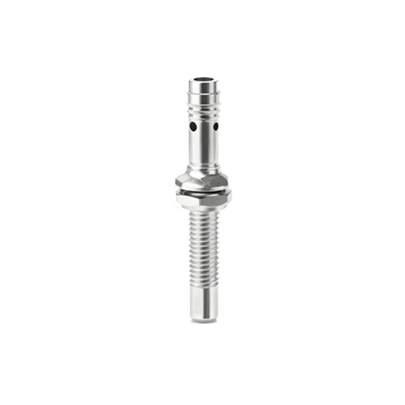
Simultaneously, the electronic circuit is prepared. The application-specific integrated circuit (ASIC) or discrete components are mounted onto a small printed circuit board (PCB) using surface-mount technology (SMT). This automated process ensures consistent soldering quality. This PCB houses the oscillator that generates the high-frequency electromagnetic field, the circuit that detects changes in this field caused by a target, and the solid-state switch (typically NPN or PNP transistor) for the output. The wound coil is then soldered onto designated points on this PCB.
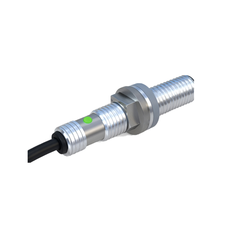
The sub-assembly—coil and PCB—is then carefully inserted into the sensor housing. A critical step follows: potting. The housing is filled with a thermally conductive, chemically resistant epoxy resin compound. This process serves multiple vital functions: it permanently secures the internal components, provides exceptional protection against vibration and mechanical shock, and creates a complete seal against contaminants like dust, oil, and coolants. The potting compound also aids in heat dissipation from the electronic components. The filled units are cured in ovens at specific temperature profiles to achieve full structural integrity.
Once cured, the sensing face is installed. For standard inductive sensors, this is often a wear-resistant plastic cap that allows the electromagnetic field to pass through while protecting the ferrite core. For factors, a metallic face of stainless steel may be used. The housing is then sealed, often with laser welding or ultrasonic sealing for IP67, IP68, or IP69K ratings, guaranteeing ingress protection.
The now-assembled sensors enter the critical phase of calibration and testing. Each unit is placed on a automated test fixture. Key parameters are verified:
1. Sensing Distance (Sn): The actual switching distance is measured against the nominal value (e.g., 5mm, 8mm). It must fall within the specified tolerance (typically ±10%).
2. Hysteresis: The difference between the switch-on and switch-off points is tested to ensure stable switching and prevent chatter.
3. Output Function: The switching state (NO/NC) and output current are verified under load.
4. Frequency Response: The maximum switching frequency is tested.
5. Environmental Tests: Sample units from the batch undergo rigorous tests, including temperature cycling, humidity exposure, and resistance to short-circuit, overload, and reverse polarity.
Sensors that pass all electrical tests are often subjected to a final "aging" or burn-in process. They are powered and cycled for a set period under elevated temperature. This stress screening helps identify and eliminate early-life failures, ensuring only robust units proceed.
The final stage is marking and packaging. The sensor body is laser-marked with its type code, electrical data, brand, and certifications (e.g., CE, UL). They are then packed in anti-static packaging, with datasheets included, and boxed for shipment.
In conclusion, the manufacturing of proximity sensors is a symphony of precision engineering, automated assembly, and uncompromising quality assurance. Each step, from coil winding to hermetic sealing and exhaustive testing, is designed to produce a component that delivers flawless, maintenance-free performance in the demanding environments of modern industry. Understanding this process underscores the value and engineering embedded in these ubiquitous devices.