In the rapidly evolving semiconductor industry, the demand for high-precision inspection technologies has never been greater. Laser sensors have emerged as a critical tool for chip detection, offering unparalleled accuracy, speed, and reliability in quality control processes. These sensors utilize focused laser beams to measure dimensions, detect defects, and verify alignment on semiconductor wafers and integrated circuits (ICs). As chip geometries shrink to nanometer scales, traditional optical or contact-based inspection methods often fall short, making non-contact laser-based solutions indispensable.
Laser sensors operate on principles such as triangulation, confocal microscopy, or interferometry. Triangulation sensors, for instance, project a laser spot onto the chip surface, with a receiver capturing the reflected light at an angle to calculate distance and surface topography. This enables real-time detection of minute imperfections like scratches, particles, or pattern deviations. Confocal laser sensors enhance resolution by using pinhole apertures to eliminate out-of-focus light, allowing for precise 3D imaging of layered structures in multi-die stacks or advanced packaging. Interferometric sensors, leveraging wave interference, excel in measuring ultra-fine surface roughness and thickness variations critical for chip performance.
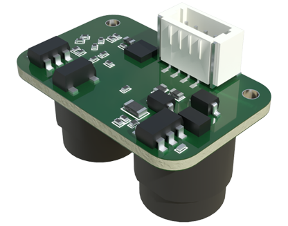
The integration of laser sensors into automated inspection systems has revolutionized semiconductor manufacturing. In fabrication plants (fabs), these sensors are deployed in-line during lithography, etching, and deposition stages. They perform tasks such as overlay alignment verification, where even sub-micron misalignments can lead to circuit failures. By providing continuous feedback, laser sensors enable adaptive process control, reducing yield loss and minimizing downtime. For example, in wafer defect inspection, high-speed laser scanners can cover entire wafers in seconds, identifying anomalies that might escape human or conventional machine vision systems.
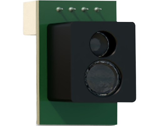
Key advantages of laser sensors include their non-destructive nature, high repeatability, and immunity to ambient light interference. Unlike contact probes, they avoid physical damage to delicate chip surfaces. Additionally, advancements in laser technology, such as the use of short-wavelength lasers (e.g., ultraviolet or blue lasers), have improved spatial resolution to below 100 nanometers. This is crucial for inspecting cutting-edge nodes like 5nm or 3nm processes, where defects as small as a few atoms can impact functionality.
However, challenges persist, including the high cost of precision laser systems and sensitivity to environmental factors like vibration or temperature fluctuations. To address these, manufacturers are developing robust sensor designs with built-in calibration and compensation algorithms. Emerging trends also incorporate artificial intelligence (AI) and machine learning (ML) with laser sensor data, enabling predictive analytics for defect classification and root-cause analysis. For instance, AI-driven laser inspection systems can learn from historical data to distinguish between critical and non-critical defects, optimizing repair processes.
In conclusion, laser sensors are pivotal in ensuring the quality and reliability of semiconductor chips. As the industry pushes toward more complex architectures like 3D-ICs and heterogeneous integration, the role of laser-based inspection will only expand. Continuous innovation in sensor technology, coupled with smart manufacturing initiatives, promises to enhance chip yields and drive the next generation of electronic devices. Engineers and fab operators must stay abreast of these developments to maintain competitive edge in a market where precision is paramount.
