Semiconductor proximity sensors represent a critical component in modern industrial automation, robotics, and smart device applications. Their production is a sophisticated process that blends materials science, precision engineering, and advanced electronics. This guide delves into the core manufacturing stages, key technologies, and industry best practices.
The production journey begins with substrate preparation, typically using silicon wafers. These wafers undergo rigorous cleaning in ultrapure environments to eliminate contaminants. The heart of the sensor lies in its sensing element, often based on Hall-effect, capacitive, or photoelectric principles. For Hall-effect sensors, epitaxial growth techniques are employed to deposit thin layers of gallium arsenide (GaAs) or indium antimonide (InSb) onto the silicon substrate. This creates the sensitive region that detects magnetic field changes from approaching ferrous objects. Photolithography and etching processes then define the microscopic circuit patterns with nanometer-scale precision.
Doping processes, such as ion implantation or diffusion, introduce specific impurities into the semiconductor material to modify its electrical properties, creating p-n junctions essential for signal generation. Following this, metallization deposits aluminum or copper interconnects to form the electrical pathways. A crucial step is the passivation layer application, usually silicon nitride or silicon dioxide, which protects the delicate semiconductor structures from moisture, dust, and mechanical damage.
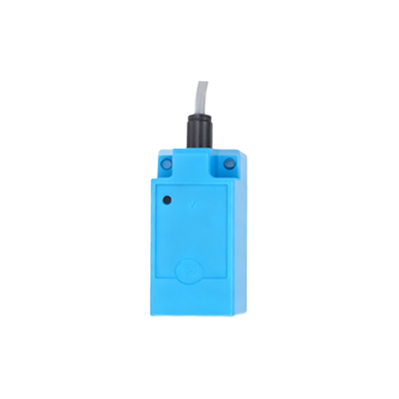
Packaging is where the die becomes a functional sensor. The semiconductor die is mounted onto a lead frame or substrate using conductive epoxy or solder. Wire bonding, utilizing gold or aluminum wires, establishes electrical connections between the die pads and the external pins. The assembly is then encapsulated in a molded plastic housing, often made from PBT or epoxy resin, which provides environmental protection and determines the sensor's form factor. For certain high-reliability applications, hermetic sealing in ceramic or metal packages is utilized.
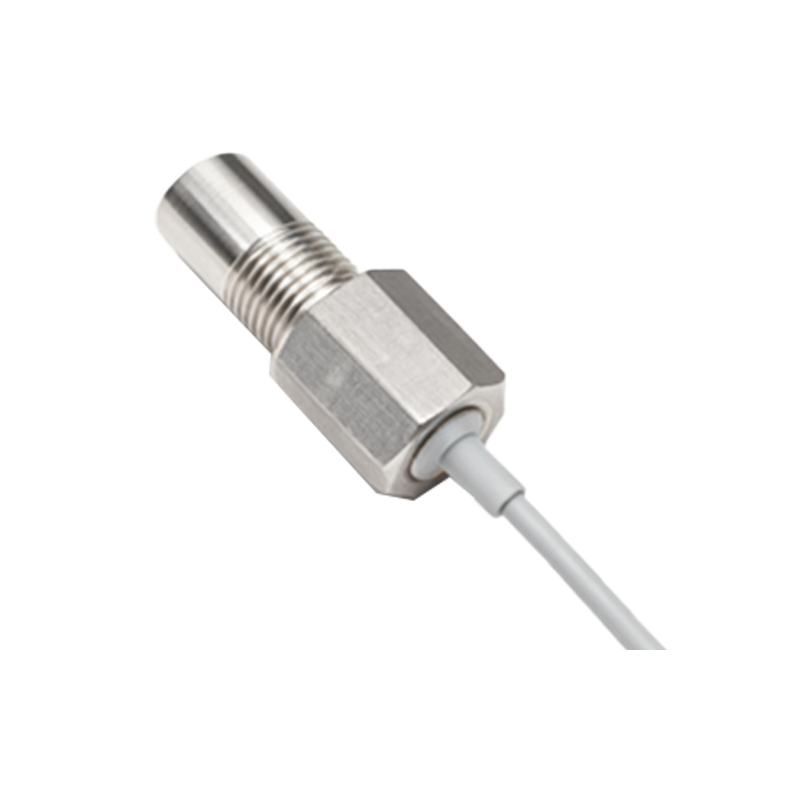
Calibration and testing are non-negotiable final stages. Each sensor undergoes automated testing to verify key parameters: sensing distance, hysteresis, response time, temperature stability, and output signal accuracy. Laser trimming may adjust resistor values on-chip to fine-tune sensitivity. Advanced production lines employ machine vision systems and automated handling to ensure consistency and high throughput.
Industry trends are pushing production towards greater miniaturization and integration. The adoption of Micro-Electro-Mechanical Systems (MEMS) technology allows for the creation of extremely small, low-power sensors. Furthermore, the integration of analog-to-digital converters (ADCs) and digital signal processing (DSP) logic onto the same chip is creating "smart sensors" that offer calibrated digital outputs and diagnostic capabilities directly from the package.
Challenges in production include managing thermal stresses during packaging, ensuring long-term stability under varying environmental conditions, and achieving cost-effective yields for high-volume applications. Adherence to international standards like IEC 60947-5-2 is paramount for quality and interoperability.
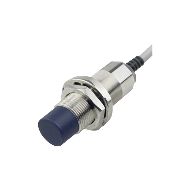
In conclusion, the production of semiconductor proximity sensors is a testament to precision manufacturing. It requires a deep understanding of semiconductor physics, meticulous process control, and relentless testing to deliver the reliability and performance demanded by today's automated systems. As Industry 4.0 advances, these sensors will continue to evolve, with production methodologies adapting to incorporate more IoT connectivity and AI-driven self-diagnostic features directly into the fabrication process.