In industrial automation and process control, proximity switch sensors are indispensable components for detecting the presence or absence of objects without physical contact. Among these, high-temperature proximity switches are specialized variants engineered to operate reliably in extreme thermal environments, such as those found in metal casting, glass manufacturing, furnace operations, and automotive engine compartments. This article delves into the schematic design and operational principles of these robust sensors, focusing on their construction, key components, and the electronic circuitry that enables stable performance under thermal stress.
The core function of a proximity switch, regardless of its operating temperature range, is to generate an electrical signal when a target object enters its sensing field. High-temperature models achieve this while withstanding ambient temperatures often exceeding 150°C, and in some cases, reaching up to 200°C or more. The schematic of such a sensor can be broadly divided into three main sections: the sensing head/oscillator circuit, the signal conditioning and evaluation circuit, and the output switching stage. Each section is designed with components and materials selected specifically for thermal resilience.
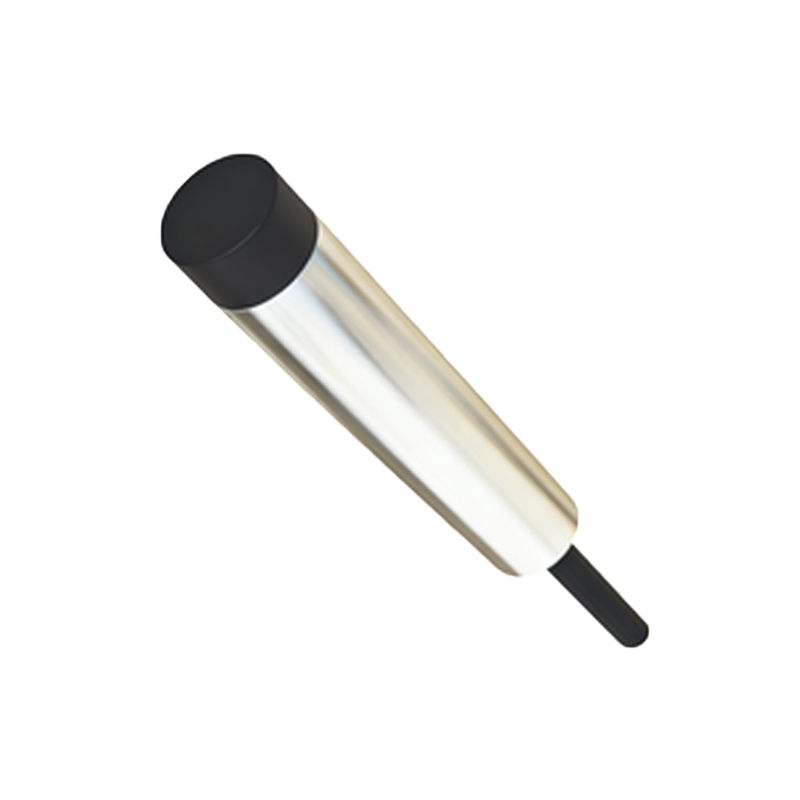
1. Sensing Head and Oscillator Circuit:
The sensing element is typically a coil that forms part of an LC resonant oscillator circuit. In inductive proximity sensors (the most common type for metal detection), this coil generates a high-frequency electromagnetic field. When a metallic target enters this field, eddy currents are induced in the target, causing a change in the oscillation amplitude or frequency within the coil. The schematic shows the coil (L1) connected with a capacitor (C1) to form the tank circuit. A dedicated oscillator IC or transistor-based circuit (e.g., using a Colpitts or Hartley oscillator configuration) drives this tank. For high-temperature applications, the coil is wound using high-temperature-rated magnet wire, and the core material (if used) must have stable magnetic properties across the temperature range. The capacitor C1 must be a high-temperature ceramic type, such as X7R or C0G (NP0) dielectric, to maintain stable capacitance.
2. Signal Conditioning and Evaluation Circuit:
The subtle change in the oscillator's signal due to target presence is too small to directly drive an output. This raw signal is first fed into an amplifier stage. The schematic includes an operational amplifier (Op-amp) configured for amplification. Critical here is the selection of an Op-amp specified for extended industrial temperature ranges (e.g., -40°C to +125°C or higher). Following amplification, the signal passes through a demodulator and filter network (involving diodes like D1, D2 and capacitors C2, C3) to convert the AC oscillation change into a smooth DC voltage level. This DC level is then compared against a predefined threshold voltage (Vref) using a comparator circuit. The threshold is often set by a voltage divider network or a precision reference IC, both utilizing high-temperature-stable resistors. When the conditioned signal exceeds Vref, the comparator toggles its output state, indicating target detection.
3. Output Switching Stage:
The digital signal from the comparator drives the final output stage. For high-temperature durability, the output switching device is crucial. While some designs use a bipolar junction transistor (BJT), a more robust and common choice is a MOSFET due to its superior switching characteristics and thermal performance. The schematic depicts an N-channel MOSFET (Q1) acting as a low-side switch. It controls the current flow through the output terminals, typically connecting to a load (e.g., a PLC input, relay, or indicator lamp). Protection components are vital: a flyback diode (D3) is placed across the load if it is inductive to suppress voltage spikes, and a series resistor (Rlimit) may be used to limit inrush current. All passive components in this stage—resistors, diodes—must be high-temperature rated.
Key Design Considerations for High-Temperature Operation:
Component Selection: Every component, from ICs and transistors to resistors, capacitors, and diodes, must have a published operating temperature range that exceeds the maximum expected ambient temperature. Semiconductor packages better suited for heat dissipation (like SOIC, DPAK) are preferred.
Thermal Management: The schematic may not explicitly show it, but the physical layout and housing are designed to dissipate heat. This includes using high-temperature printed circuit board (PCB) materials (e.g., polyimide or ceramic substrates), minimizing power dissipation in active components, and employing thermally conductive potting compounds or heatsinks where necessary.
Stability Compensation: Temperature drift can affect oscillator frequency, amplifier gain, and reference voltages. The schematic often incorporates temperature compensation techniques. This can involve using components with opposing thermal coefficients (e.g., pairing specific resistors) or utilizing ICs with built-in compensation.
Power Supply Regulation: A stable power supply is paramount.