In the rapidly evolving field of electrical engineering, the synergy between image sensors and laser technology is driving innovation across numerous applications. This article delves into the fundamental principles, key technologies, and integrated applications of these two critical components, providing a detailed technical overview for professionals and enthusiasts alike.
Image sensors, primarily Charge-Coupled Devices (CCDs) and Complementary Metal-Oxide-Semiconductor (CMOS) sensors, are the electronic eyes of modern systems. They convert incoming light (photons) into electrical signals (electrons). The core process involves a photodiode array where each pixel captures light intensity. CCD sensors, known for high quality and low noise, transfer charge across the chip to a single output node. In contrast, CMOS sensors, which have become dominant due to lower power consumption, higher integration, and faster readout speeds, perform charge-to-voltage conversion at each pixel. Key performance metrics include resolution, pixel size, dynamic range, signal-to-noise ratio (SNR), and quantum efficiency. Recent advancements like Back-Side Illumination (BSI) and stacked sensor designs have significantly improved light sensitivity and functionality in compact form factors.
Laser technology, an acronym for Light Amplification by Stimulated Emission of Radiation, provides coherent, monochromatic, and highly directional light beams. Lasers operate on the principle of population inversion within a gain medium (solid-state, gas, diode, or fiber). When excited by an external energy source, photons stimulate the emission of more photons, creating an amplified light beam. Key laser types include semiconductor laser diodes, which are compact and efficient, and fiber lasers, known for high power and beam quality. Critical parameters are wavelength (ranging from ultraviolet to far-infrared), output power, beam divergence, coherence length, and modulation capability. Pulsed lasers, such as Q-switched or mode-locked lasers, generate extremely short, high-peak-power pulses crucial for many sensing and imaging applications.

The convergence of these technologies is where transformative applications emerge. One prime example is Laser Radar (LiDAR) for autonomous vehicles and 3D mapping. A laser diode emits rapid pulses of light towards a target. The reflected light is captured by a highly sensitive image sensor, often a Single-Photon Avalanche Diode (SPAD) array or a specialized CMOS sensor. By precisely measuring the time-of-flight (ToF) of each pulse, the system constructs a detailed, real-time 3D point cloud of the environment. This requires precise synchronization between the nanosecond laser pulses and the sensor's detection circuitry.
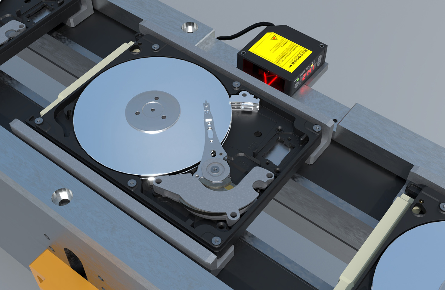
In industrial machine vision, structured light scanning uses laser projectors to cast precise patterns (lines, grids) onto objects. A high-speed CMOS camera captures the distorted pattern, and sophisticated algorithms compute depth and surface topography for quality inspection, robotic guidance, and reverse engineering. Here, the laser provides the controlled illumination, while the image sensor captures the high-contrast pattern with minimal motion blur.
Biomedical imaging heavily relies on this synergy. Confocal microscopy and Optical Coherence Tomography (OCT) use low-coherence lasers as light sources. In OCT, for instance, light reflected from biological tissues interferes with a reference beam. The resulting interference pattern is detected by a spectrometer (using a line-scan image sensor) or a photodiode array, enabling micron-resolution, cross-sectional imaging of the retina or skin layers non-invasively.
Laser-based communication systems, including Free-Space Optical (FSO) links, utilize laser diodes for data transmission. On the receiver end, an image sensor or an avalanche photodiode (APD) acts as the detector. Advanced systems might use sensor arrays to mitigate atmospheric turbulence by employing multiple-input, multiple-output (MIMO) techniques.
Material processing and sensing also benefit. In laser-induced breakdown spectroscopy (LIBS), a high-power pulsed laser ablates a material sample, creating a micro-plasma. The emitted plasma light, characteristic of the elemental composition, is dispersed by a spectrometer and captured by an image sensor (ICCD or CCD) for precise chemical analysis.
Designing systems that integrate lasers and image sensors presents significant engineering challenges. These include managing optical alignment, minimizing stray light and laser speckle, synchronizing high-speed pulses with sensor exposure (gating), and handling the vast data throughput from high-resolution, high-frame-rate sensors. Thermal management for both high-power lasers and densely packed sensor arrays is critical for stability and longevity. Furthermore, eye safety regulations (IEC 60825) strictly govern the use of lasers, especially in consumer-facing applications like LiDAR.
The future points toward deeper integration and miniaturization. Emerging trends include the development of silicon photonics, where optical components (including lasers and waveguides) are fabricated on silicon chips alongside electronic CMOS sensors, promising ultra-compact, low-cost systems. Quantum image sensors that can detect single photons with high timing resolution will revolutionize low-light and secure communication applications. Similarly, frequency comb lasers offer unprecedented precision for spectroscopic sensing when paired with advanced detectors.
In conclusion, image sensors and lasers are not standalone technologies but are fundamentally interdependent in modern electro-optical systems. The continuous advancement in CMOS sensor technology, coupled with innovations in laser diode efficiency, wavelength diversity, and pulsed operation, is unlocking new capabilities. For electrical engineers, a robust understanding of both domains—from semiconductor physics and optics to signal processing and system integration—is essential to pioneer the next generation of devices in automation, healthcare, communications, and scientific discovery. The precise interplay of controlled light emission and sophisticated light detection remains a cornerstone of technological progress.