In modern industrial automation, laser sensor modules have become indispensable components for precision measurement, object detection, and quality control. A comprehensive understanding of laser sensor module schematics is crucial for engineers and technicians involved in system design, integration, and maintenance. This article delves into the typical schematic diagram of a standard industrial laser sensor module, explaining each functional block and its role in ensuring reliable operation.
A standard laser sensor module schematic can generally be divided into several key sections: the laser diode driver circuit, the optical transmission and reception path, the photodetector and signal conditioning circuitry, the microcontroller or signal processing unit, and the output interface stage.
The heart of the module is the laser diode driver circuit. This section is responsible for providing a stable, regulated current to the laser diode. It often includes constant current sources, protection diodes, and thermal compensation elements to prevent current spikes and overheating, which are critical for maintaining diode longevity and consistent optical output power. Precise current control directly influences the stability and accuracy of the emitted laser beam.
The optical path is represented in schematics by symbols indicating the laser diode, collimating lenses, and sometimes beam splitters or focusing optics. The emitted light travels toward the target. The reflected or diffused light is then collected by a receiving lens system, which focuses it onto the photodetector, typically a photodiode or a position-sensitive device (PSD). In triangulation-based sensors, the schematic will show the precise angular relationship between the emitter, the target, and the receiver.

The photodetector circuit is a critical stage for converting faint optical signals into usable electrical signals. It consists of the photodetector itself, followed by a transimpedance amplifier (TIA) that converts the photocurrent into a voltage. This stage often includes filtering components (low-pass or band-pass filters) to suppress ambient light noise and electrical interference. High-gain, low-noise amplifier stages are essential here to achieve a good signal-to-noise ratio, especially for long-range or low-reflectivity targets.

The conditioned analog signal is then fed into the signal processing unit. In digital modules, this is typically a microcontroller (MCU) or a dedicated digital signal processor (DSP). The schematic will show the MCU/DSP along with its supporting circuitry: a stable clock crystal, reset circuit, voltage regulators, and memory (EEPROM for calibration data). This unit digitizes the analog signal via an analog-to-digital converter (ADC), either internal or external. It then executes algorithms to calculate distance, presence, or profile based on the received signal's timing, intensity, or positional data on the PSD. Calibration parameters stored in memory are applied here to ensure accuracy.
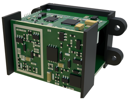
Finally, the output interface circuit prepares the processed data for communication with a host controller like a PLC. Common outputs include digital switching (NPN/PNP transistors for open-collector outputs), analog voltage/current (0-10V, 4-20mA via precision op-amp circuits), and serial communication interfaces (RS-232, RS-485, or IO-Link transceiver chips). The schematic details the output transistors, protection diodes for back-EMF, and isolation optocouplers if the module features galvanic isolation for noise immunity.
Power supply conditioning is another vital part of the schematic. An industrial laser sensor must operate reliably from a wide-range DC supply (e.g., 10-30V DC). The schematic will show input protection (fuse, polarity protection diode), a switching or linear voltage regulator to create stable internal voltages (e.g., 5V, 3.3V), and sufficient decoupling capacitors near each IC.
When analyzing a schematic, engineers should pay close attention to component ratings, especially for the laser driver and output stages, and the layout of ground planes to minimize noise. Understanding the interplay between these blocks allows for effective troubleshooting—for instance, diagnosing weak signals by checking the photodetector amp stages or output errors by verifying the MCU and its communication lines.
In summary, a laser sensor module schematic is a blueprint that reveals the sophisticated synergy between optics, analog electronics, and digital processing. Mastery of its interpretation empowers professionals to deploy, maintain, and innovate with these precise tools, driving efficiency and quality in automated industrial environments.