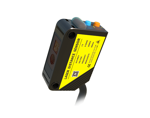
In the rapidly evolving landscape of industrial automation, precision sensing technology stands as a cornerstone of innovation and efficiency. Among the myriad of sensing solutions available, laser-based sensors have carved out a critical niche due to their unparalleled accuracy, speed, and reliability. The development of a dedicated Laser Sensor Development Board represents a significant leap forward, providing engineers and system integrators with a powerful, flexible platform to prototype, test, and deploy advanced sensing applications. This article delves into the architecture, key features, and practical applications of a state-of-the-art laser sensor development board designed for the demanding environments of modern industry.
At its core, a modern laser sensor development board integrates several critical subsystems into a cohesive unit. The primary component is the laser emitter, typically a Class 2 or Class 3R laser diode operating in the visible red or infrared spectrum. This is paired with a high-sensitivity photodetector or a position-sensitive device (PSD) to capture the reflected light. The true intelligence of the board lies in its signal processing unit, which is often built around a high-performance microcontroller (MCU) or a digital signal processor (DSP). This processor runs sophisticated algorithms for tasks such as time-of-flight (ToF) calculation, triangulation-based distance measurement, or laser line profiling. The board is equipped with various communication interfaces, including UART, I2C, SPI, and industrial protocols like Modbus or Ethernet/IP, ensuring seamless integration into larger control systems. Robust power management circuitry, input/output (I/O) ports for triggers and alarms, and often an onboard display or status LEDs complete the hardware package.
The software ecosystem accompanying the development board is equally vital. Manufacturers typically provide comprehensive software development kits (SDKs), libraries, and application programming interfaces (APIs). These tools allow developers to customize measurement parameters, filter noise, calibrate the sensor for specific surfaces or materials, and implement application-specific logic without needing to delve into low-level hardware programming. Many boards support popular embedded development environments, facilitating a streamlined workflow from concept to functional prototype.
The applications for such a development board are vast and transformative across multiple sectors. In factory automation, it enables the creation of precise non-contact measurement systems for part inspection, dimensional gauging, and assembly verification. Robots equipped with laser sensors developed on these boards gain enhanced capabilities for object detection, bin picking, and precise navigation. In logistics and warehousing, laser sensors are pivotal for palletizing, dimensioning packages, and automated guided vehicle (AGV) guidance. Furthermore, in sectors like agriculture, construction, and aerospace, these boards serve as the foundation for developing specialized equipment for terrain mapping, structural alignment, and defect detection.
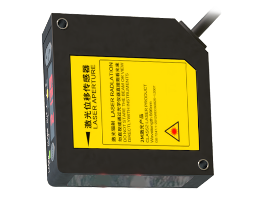
Developing with a laser sensor board does present certain challenges that engineers must navigate. Laser safety is paramount; ensuring designs comply with international standards like IEC 60825 is non-negotiable. Environmental factors such as ambient light interference, dust, and varying surface reflectivity can affect performance, necessitating intelligent software compensation. Additionally, achieving sub-micron or sub-millimeter accuracy requires careful calibration and a deep understanding of optical principles. However, the modularity and programmability of a dedicated development board significantly lower these barriers, allowing teams to iterate quickly and focus on solving the application problem rather than the underlying sensor physics.
Looking ahead, the trajectory for laser sensor development boards points toward greater integration, intelligence, and connectivity. Future iterations will likely incorporate more onboard processing power to handle edge computing tasks, integrate machine learning cores for adaptive sensing, and feature enhanced cybersecurity for connected industrial IoT applications. The convergence of high-speed data interfaces and miniaturized optical components will also enable more compact and versatile form factors.
In conclusion, a dedicated Laser Sensor Development Board is an indispensable tool for engineers pushing the boundaries of industrial sensing and automation. By abstracting the complexities of laser optics and low-level signal processing, it accelerates the development cycle, fosters innovation, and empowers the creation of smarter, more responsive, and more efficient automated systems. As Industry 4.0 continues to mature, the role of such flexible development platforms will only become more central in bridging the gap between cutting-edge sensor technology and real-world industrial solutions.