Proximity displacement sensors are fundamental components in modern industrial automation, offering non-contact measurement of object position and displacement. These sensors operate based on electromagnetic, capacitive, or inductive principles, with inductive proximity sensors being the most prevalent in industrial applications due to their robustness and reliability. This article delves into the schematic design and operational mechanics of a standard inductive proximity displacement sensor, providing a detailed technical overview for engineers and industry professionals.
The core of an inductive proximity sensor comprises an oscillator circuit, a demodulator, a trigger circuit, and an output stage. The schematic begins with the oscillator, typically built around a Colpitts or Hartley configuration using a transistor or an integrated oscillator IC. This circuit generates a high-frequency electromagnetic field (usually in the range of 100 kHz to 1 MHz) at the sensor's active face, which is created by a coiled inductor. When a metallic target enters this oscillating field, eddy currents are induced on the target's surface. These eddy currents draw energy from the oscillator, resulting in a measurable attenuation or damping of the oscillation amplitude.
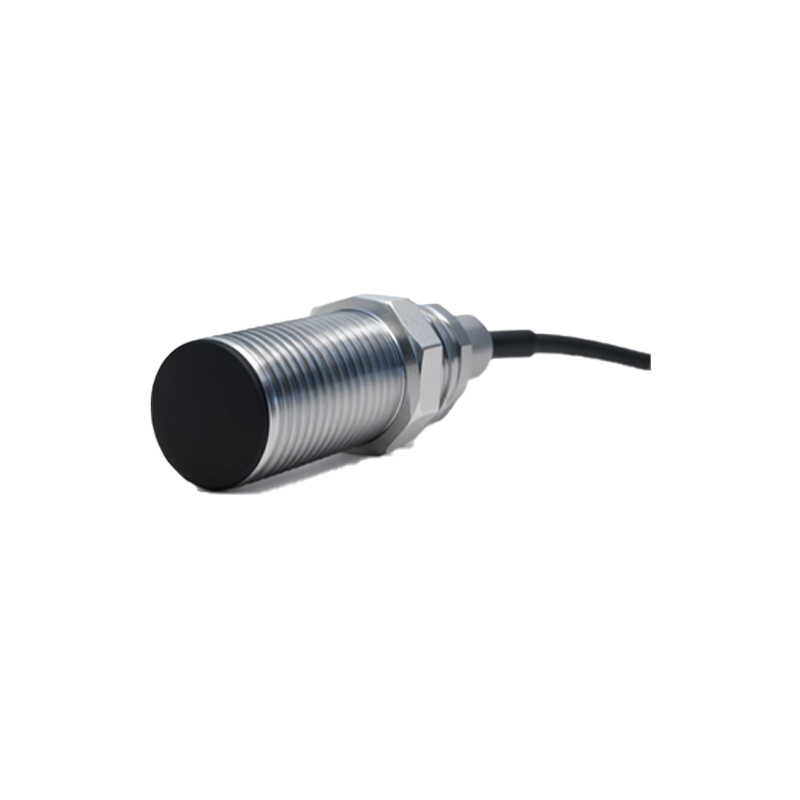
The demodulator circuit, often a simple diode-based peak detector or a more sophisticated synchronous demodulator, converts the damped AC signal from the oscillator into a corresponding DC voltage level. This DC signal is proportional to the distance between the sensor and the target—closer proximity causes greater damping and a lower DC voltage. This analog signal is then fed into a trigger circuit, commonly a Schmitt trigger configured with operational amplifiers or a dedicated comparator IC. The Schmitt trigger provides hysteresis, preventing output oscillation when the input signal is near the threshold. It compares the demodulated DC voltage against a predefined reference voltage. Once the signal crosses the threshold (indicating the target is within the specified sensing range), the trigger circuit switches state.
Following the trigger, the output stage activates. In a typical NPN or PNP transistor output schematic, the trigger drives the base of the output transistor, allowing current to flow from the collector to the emitter, thus switching the load connected to the sensor. For analog output variants, the demodulated DC signal is instead conditioned through an amplifier and buffer circuit to provide a continuous voltage (e.g., 0-10V) or current (e.g., 4-20mA) output linearly proportional to displacement. The schematic also includes essential protective components: a polarity protection diode at the power supply inputs, a Zener diode for voltage regulation, and RC snubber networks or transient voltage suppression diodes to protect against voltage spikes and electromagnetic interference (EMI), ensuring durability in harsh industrial environments.
Key design considerations in the schematic involve selecting the oscillator frequency and coil geometry to optimize sensing range and sensitivity for specific metals. Shielding is crucial; a ferrite core or a metal shield around the coil confines the electromagnetic field, making the sensor less susceptible to sideward metal interference and enabling flush mounting. The choice of output type (digital switching or analog) and wiring configuration (2-wire, 3-wire, or 4-wire) is also defined in the schematic, impacting integration with programmable logic controllers (PLCs) and other control systems.
In practice, understanding this schematic allows engineers to troubleshoot sensor failures, such as inconsistent switching caused by a failing oscillator component or degraded output due to a damaged protection diode. It also informs selection criteria: for high-speed applications, a sensor with a fast-switching oscillator and minimal hysteresis is chosen, while for applications involving different metals, a sensor with a frequency-dependent response curve must be selected. Ultimately, the proximity displacement sensor schematic represents a elegant synthesis of electromagnetic theory and practical electronic design, enabling precise, wear-free measurement critical for positioning, inspection, and automation tasks across manufacturing, robotics, and automotive industries.