Proximity sensors are critical components in modern automation, industrial control, and safety systems. Their manufacturing process is a sophisticated blend of precision engineering, material science, and rigorous quality control. This article delves into the detailed production workflow, from raw material selection to final testing, providing electrical engineers with a thorough understanding of how these essential devices are made.
The journey begins with the design and prototyping phase. Engineers utilize CAD software to model the sensor, defining its form factor, sensing range (inductive, capacitive, or photoelectric), and output type (PNP, NPN, analog, or IO-Link). The core component, the sensing element, is designed first. For inductive sensors, this involves designing a coil and oscillator circuit. The coil is typically wound from high-grade copper wire, and its characteristics are meticulously calculated to achieve the desired sensing distance and frequency response. Prototypes are then built and subjected to initial functional and environmental tests to validate the design.
Following design validation, the process moves to Printed Circuit Board (PCB) fabrication. A multi-layer PCB is manufactured, featuring the oscillator, amplifier, signal conditioner, and output switching circuitry. Surface-mount technology (SMT) lines populate the board with micro-components like resistors, capacitors, integrated circuits, and the crucial ASIC (Application-Specific Integrated Circuit) that often houses the core logic. Reflow soldering ensures reliable electrical connections. The quality of this assembly is paramount, as it dictates the sensor's stability and noise immunity.
Concurrently, the housing and sensing face are produced. For industrial-grade sensors, housings are typically molded from rugged materials like nickel-plated brass, stainless steel, or engineering plastics such as PBT or PPS. These materials offer excellent resistance to chemicals, oils, and mechanical impact. The molding process, often injection molding for plastics or machining/die-casting for metals, must achieve tight tolerances to ensure IP67/IP69K ingress protection ratings. The sensing face, a critical area, is made from a material that allows the electromagnetic field (for inductive types) or light beam (for photoelectric types) to pass through effectively, often a specific grade of epoxy or ceramic.
The next stage is coil winding and assembly for inductive sensors. Automated winding machines precisely wind the copper wire around a ferrite core to form the oscillator coil. This sub-assembly is then potted, or encapsulated, with a specialized epoxy resin. Potting serves multiple purposes: it secures the coil mechanically, protects it from moisture, vibration, and contaminants, and critically, it fixes the coil's electrical parameters, ensuring consistent sensing performance. The potted coil assembly is then integrated with the PCB.
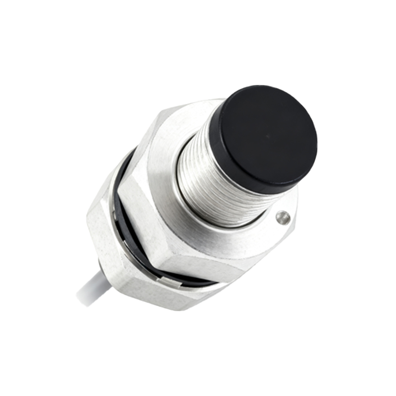
Final assembly involves carefully placing the PCB into the housing. The potted sensing element is aligned precisely with the sensing face. All internal connections are made, and the housing is sealed, often using laser welding, ultrasonic welding, or chemical bonding with O-rings to achieve a hermetic seal. For connectors, either integrated M8/M12 styles or cable outlets are fitted and sealed. This step is performed in a controlled environment to prevent dust contamination.
Quality assurance is not a single step but an integral part of the entire process. Incoming materials are inspected. During PCB assembly, Automated Optical Inspection (AOI) checks solder joint quality. Post-assembly, every sensor undergoes a battery of tests. These include:
1. Functional Testing: Sensors are cycled on and off using target materials at specified distances to verify switching accuracy, hysteresis, and repeatability.
2. Electrical Testing: Parameters like operating voltage range, current consumption, output leakage current, and short-circuit protection are verified.
3. Environmental Testing: Samples from each batch are subjected to temperature cycling, humidity tests, vibration, and shock tests to ensure reliability under harsh conditions.
4. Endurance Testing: Sensors are activated for millions of cycles to validate mechanical and electrical longevity.
Finally, calibrated and tested sensors are labeled with their technical specifications, branded, and packaged for shipment. The entire process is governed by quality management systems like ISO 9001, ensuring traceability and continuous improvement.
For electrical engineers, understanding this process underscores the importance of selecting sensors from manufacturers with robust, vertically integrated production capabilities. It highlights why specifications like temperature rating, housing material, and protection class are not just datasheet numbers but the result of deliberate engineering and manufacturing choices. This knowledge empowers engineers to make informed decisions when integrating proximity sensors into demanding applications, from automotive assembly lines to food processing plants, ensuring system reliability and longevity.