In the realm of high-precision industrial measurement, laser displacement sensors represent the pinnacle of non-contact metrology technology. Among these, the most expensive models stand apart, not merely due to their price tags, which can soar into the tens of thousands of dollars, but because of the extraordinary engineering, unparalleled performance, and specialized applications they enable. These sensors are not general-purpose tools; they are highly specialized instruments designed for mission-critical tasks where micron or even sub-micron accuracy is non-negotiable.
The core value proposition of these premium sensors lies in their exceptional specifications. They achieve staggering resolutions down to 0.01 micrometers, repeatability in the nanometer range, and sampling speeds exceeding 500 kHz. This performance is built upon several key technological pillars. First is the laser source itself. Top-tier sensors utilize ultra-stable, short-wavelength lasers (often blue or violet) with perfectly collimated beams. This minimizes optical diffraction effects, allowing for precise measurement on edges, small features, and challenging surfaces like transparent glass or shiny metals that would confound standard red laser sensors.
Second is the advanced optical system and detector. The most sophisticated models employ confocal chromatic or spectral interferometry principles rather than simple triangulation. Confocal chromatic sensors, for instance, use white light that is focused to a specific point by a multi-lens optical system. Only the wavelength perfectly focused on the target surface is reflected back to the spectrometer, providing absolute distance measurement with exceptional immunity to surface tilt, color, or texture. This technology is inherently complex and costly to manufacture but delivers unmatched reliability for measuring steps, thicknesses, and delicate materials.
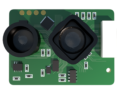
Third is the integrated computational intelligence and environmental hardening. The onboard processor performs real-time compensation for temperature drift, vibration, and other ambient factors that could degrade accuracy. The housing is typically crafted from super-invar or similar thermally stable materials, and the internal components are isolated from stress. Communication interfaces are industrial-grade, supporting high-speed Ethernet protocols like EtherCAT for seamless integration into automated production lines for 100% inline inspection.
The applications justifying such investment are found in industries where failure is not an option. In semiconductor manufacturing, these sensors measure wafer warpage, film thickness, and bump heights with nanometer precision, directly impacting chip yield. In aerospace, they verify the surface profile of turbine blades and composite materials, ensuring safety and performance. Advanced automotive R&D uses them to calibrate fuel injection nozzles and inspect critical engine components. In precision optics, they characterize lens curvatures and guide complex polishing processes.

Furthermore, the total cost of ownership extends beyond the initial purchase. It includes proprietary software suites for advanced data analysis, calibration services traceable to national standards, and dedicated technical support from application engineers. Manufacturers of these elite sensors, such as Keyence (with its LK-HD series), Micro-Epsilon (confocalDT series), and OptoNCDT, provide comprehensive solutions tailored to specific industrial challenges.
Ultimately, the world's most expensive laser displacement sensors are marvels of optoelectronics and precision engineering. They are the definitive tools for pushing the boundaries of what is measurable, enabling innovation in fields that define technological progress. Their value is not in their cost but in the critical data they provide—data that ensures quality, drives efficiency, and makes the impossible, possible in modern manufacturing and research.