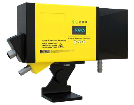
In the rapidly evolving landscape of industrial manufacturing, laser engraving has emerged as a pivotal technology for sensor production, offering unparalleled precision, durability, and efficiency. Sensors, as critical components in automotive, aerospace, medical devices, and consumer electronics, demand exacting standards for marking and identification. Laser engraving meets these demands by enabling high-resolution, permanent markings on various sensor materials—including metals, ceramics, and polymers—without compromising structural integrity.
The process utilizes focused laser beams, typically from fiber or UV lasers, to remove surface material or alter its properties, creating clear, legible engravings such as serial numbers, barcodes, logos, and calibration data. Unlike traditional methods like mechanical etching or ink printing, laser engraving is non-contact, minimizing the risk of damage to delicate sensor components. This is especially crucial for micro-sensors and MEMS (Micro-Electro-Mechanical Systems), where even minor physical stress can affect performance. Moreover, laser systems offer exceptional consistency and repeatability, ensuring every sensor meets quality control standards in high-volume production lines.
One of the key advantages of laser engraving for sensors is its adaptability to complex geometries and small form factors. Advanced galvanometer scanners and precision optics allow for rapid, programmable marking on curved or uneven surfaces, which is common in sensor housings. This flexibility reduces setup times and enhances throughput, making it ideal for just-in-time manufacturing environments. Additionally, laser-engraved markings are highly resistant to environmental factors like abrasion, heat, and chemicals, ensuring long-term readability—a critical requirement for sensors used in harsh conditions, such as industrial machinery or outdoor installations.
From an engineering perspective, the choice of laser parameters—wavelength, power, pulse duration, and scanning speed—is tailored to the sensor material to achieve optimal results. For instance, infrared lasers are effective for metals, while UV lasers are preferred for plastics and ceramics due to their "cold" processing that minimizes thermal distortion. This customization prevents issues like micro-cracking or discoloration, preserving sensor functionality. Furthermore, laser engraving supports traceability and compliance with industry regulations, such as ISO standards, by providing permanent, tamper-proof identifiers that facilitate tracking throughout a product's lifecycle.
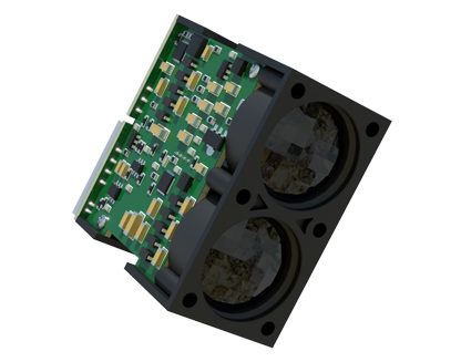
Innovations in laser technology continue to push boundaries in sensor applications. Ultrafast picosecond and femtosecond lasers enable sub-micron precision for nano-sensors, while integrated vision systems allow for real-time alignment and inspection, reducing error rates. As Industry 4.0 drives demand for smart sensors with embedded data, laser engraving can even create functional microstructures, such as diffraction gratings or conductive traces, expanding beyond mere marking. In summary, laser engraving represents a cornerstone of modern sensor manufacturing, combining technical excellence with operational efficiency to support the next generation of intelligent devices.