In the rapidly evolving landscape of industrial automation and precision measurement, laser sensor development boards have emerged as indispensable tools for engineers and developers. These boards serve as the foundational platform for prototyping, testing, and integrating laser-based sensing technologies into a wide array of applications, from robotics and autonomous vehicles to quality control and medical devices. This guide delves into the core components, selection criteria, and practical implementation strategies for these powerful development tools.
At its heart, a laser sensor development board is a printed circuit board (PCB) that integrates a laser emitter, a photodetector or sensor array, and the necessary supporting electronics. The primary function is to project a laser beam onto a target and measure the reflected light to determine parameters such as distance, displacement, presence, or profile. Key components typically include the laser diode driver circuit, which ensures stable and safe operation of the laser source; the optical receiver circuitry, often involving transimpedance amplifiers (TIAs) to convert the tiny photocurrent into a measurable voltage; and a microcontroller unit (MCU) or digital signal processor (DSP). This MCU/DSP handles signal processing, data interpretation, and communication via standard interfaces like I2C, SPI, UART, or USB.
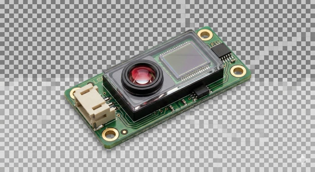
When selecting a development board, engineers must consider several critical specifications. The type of laser sensor is paramount: time-of-flight (ToF) boards measure the round-trip time of a laser pulse for distance ranging, while triangulation boards use geometric principles for high-precision displacement measurements. Other types include laser curtain boards for presence detection and LIDAR development kits for 3D mapping. Key performance parameters include measurement range, resolution, accuracy, sampling rate, and the laser's wavelength (common are 650nm red lasers and 850nm infrared). The operating environment—encompassing factors like ambient light immunity, temperature range, and potential exposure to dust or moisture—also heavily influences board selection. Furthermore, the quality of the software development kit (SDK), available libraries, and documentation can drastically reduce development time.
The practical workflow begins with understanding the board's schematic and pinout. Engineers typically connect the board to a host computer or embedded system, install necessary drivers and IDE plugins, and run initial example codes provided by the manufacturer. Calibration is a crucial step, often involving setting a known reference distance or surface to ensure measurement fidelity. From there, developers can modify firmware to filter noise, implement custom algorithms for edge detection or object classification, and integrate the sensor data with other system components like motor controllers or graphical user interfaces.
One of the most significant advantages of using a development board is the ability to rapidly prototype and debug. Engineers can test the sensor's behavior under real-world conditions before committing to a custom PCB design. For instance, in a robotic arm application, a ToF development board can be used to fine-tune the stopping distance algorithm. In a manufacturing setting, a triangulation board can be prototyped to measure the thickness of materials on a conveyor belt. The modular nature of these boards allows for quick swapping of sensor heads or upgrading the processing unit.
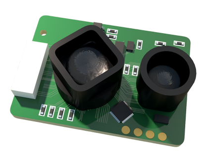
However, challenges exist. Electrical noise from other system components can interfere with sensitive analog signals from the photodetector. Proper board layout, shielding, and grounding practices are essential. Optical challenges include dealing with highly reflective or absorbent surfaces, which can distort measurements. The software must account for these anomalies through advanced filtering and compensation algorithms. Power management is another consideration, especially for battery-operated portable devices, requiring efficient laser pulsing and sleep modes.
Looking ahead, the trend in laser sensor development boards is toward higher integration, lower power consumption, and smarter onboard processing. Boards with integrated AI accelerators for real-time object recognition are becoming available. Furthermore, the rise of modular and open-source hardware platforms is fostering a collaborative environment where engineers can share custom firmware and hardware extensions.
In conclusion, a laser sensor development board is more than just an evaluation kit; it is a sandbox for innovation. It bridges the gap between sensor datasheet specifications and a fully functional, reliable system component. By carefully selecting the appropriate board based on application requirements and leveraging its full suite of development tools, engineers can accelerate the design cycle, mitigate risks, and unlock the full potential of laser sensing technology to create smarter, more precise, and autonomous systems. Mastery of these platforms is becoming a key competency in the toolkit of the modern electrical and embedded systems engineer.