In the realm of modern electronics, the seamless interaction between humans and machines is often facilitated by an unseen, yet critical component: the proximity sensor. At the core of these sophisticated sensors lies a fundamental building block—the proximity sensor wafer. This thin slice of semiconductor material, typically silicon, serves as the substrate upon which intricate circuits and sensing elements are fabricated, enabling devices to detect the presence, absence, or distance of nearby objects without physical contact.
The manufacturing journey of a proximity sensor wafer begins in ultra-clean facilities known as fabs. High-purity silicon crystals are grown and then sliced into wafers using precise diamond-edged saws. These wafers undergo a series of complex photolithography, etching, doping, and deposition processes. For proximity sensors, specific structures like photodiodes for infrared-based detection or capacitive plates for electric field sensing are patterned onto the wafer surface. The choice of technology—infrared (IR), inductive, capacitive, or ultrasonic—dictates the exact materials and design layers integrated. For instance, IR proximity sensors require the precise integration of an IR LED emitter and a photodiode receiver on the same wafer or in close proximity within the final package.
The performance and reliability of the final sensor are directly determined at the wafer level. Key parameters such as sensitivity, detection range, response time, and power consumption are engineered into the silicon. Advanced wafer-level packaging (WLP) techniques are increasingly employed, where protective caps, filters (like infrared pass filters), and even micro-lenses are added directly onto the wafer before it is diced into individual chips. This miniaturization is crucial for the ever-shrinking form factors of smartphones, tablets, wearables, and IoT devices. The infrared proximity sensor that manages your phone's display during a call, preventing accidental screen touches, originates from such a wafer.
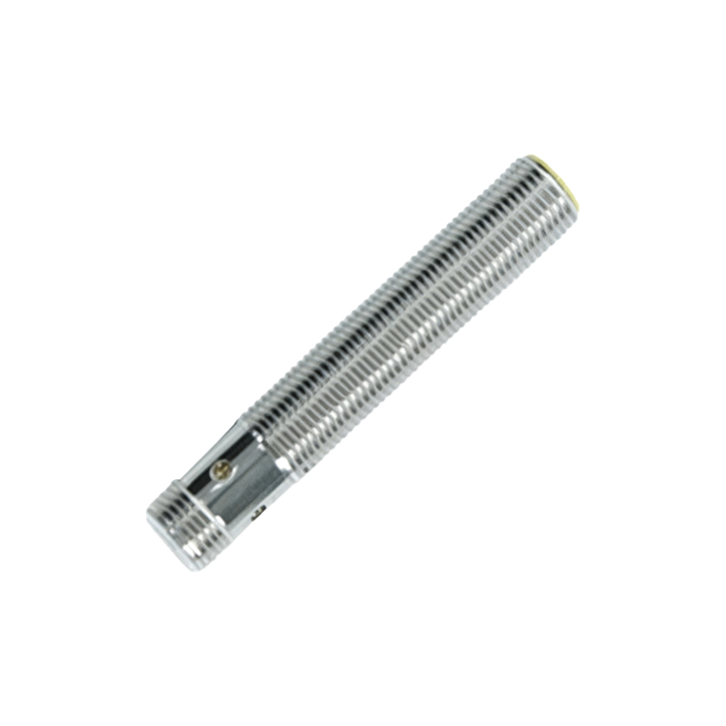
Beyond consumer electronics, proximity sensor wafers are vital in automotive applications, enabling features like hands-free trunk opening, occupancy detection, and touchless control panels. In industrial automation, they provide non-contact object detection for robotics and assembly lines, improving safety and efficiency. The medical field utilizes them in equipment for fluid level sensing and touchless interfaces in sterile environments.
The evolution of these wafers is closely tied to broader semiconductor trends. The move towards larger wafer diameters (200mm and 300mm) improves manufacturing efficiency and reduces cost per chip. Furthermore, the integration of proximity sensing with other functions—such as ambient light sensing, 3D imaging, or environmental monitoring—onto a single "combo-sensor" chip is a growing trend. This sensor fusion, fabricated on a shared wafer, enables more intelligent and context-aware devices.
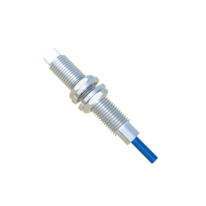
However, challenges persist. Designing for ultra-low power consumption is paramount for battery-operated devices. Shielding the sensitive circuitry from electromagnetic interference (EMI) at the wafer level is another critical design consideration. Additionally, calibrating each sensor die for consistent performance across millions of units requires sophisticated testing protocols during and after wafer fabrication.
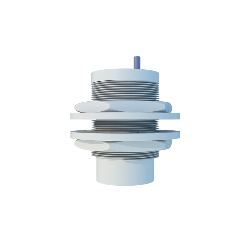
Looking ahead, innovations in materials beyond silicon, such as gallium arsenide for specific IR applications, and advanced 3D stacking of wafer layers, promise even smaller, more powerful, and more energy-efficient proximity sensors. As the demand for intuitive human-machine interfaces and smart automation continues to surge, the humble proximity sensor wafer will remain an indispensable and continuously evolving enabler, quietly powering the responsive and intelligent world around us.