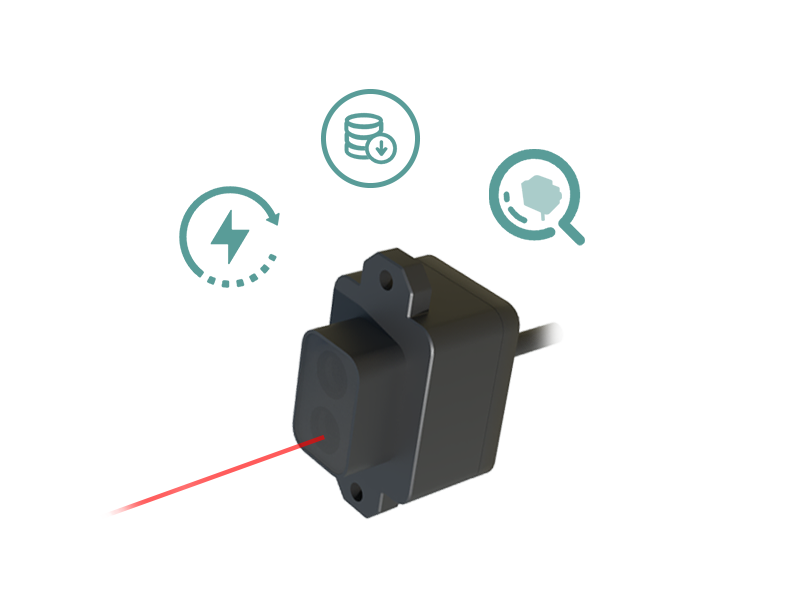
In the rapidly evolving landscape of industrial automation and IoT, sensors serve as the critical nerve endings, capturing data that drives decision-making and operational efficiency. Among the myriad of technologies employed in sensor manufacturing, laser marking has emerged as a superior method for applying permanent identification, branding, and data codes directly onto sensor components. This process, often referred to as laser engraving or etching, utilizes a focused beam of light to alter the surface of materials such as metals, ceramics, and certain plastics, creating high-contrast, indelible marks without compromising the structural integrity of the part.
The advantages of laser marking for sensors are multifaceted. Primarily, it ensures exceptional traceability. Each sensor can be marked with a unique serial number, QR code, Data Matrix, or barcode. This permanent identifier allows for precise tracking throughout the entire product lifecycle—from manufacturing and quality control to installation, maintenance, and potential recall. In industries like automotive, aerospace, and medical devices, where component history is paramount for safety and compliance, this level of traceability is non-negotiable. Unlike inkjet printing or labels, which can fade, smudge, or peel, laser marks are resistant to abrasion, chemicals, heat, and UV exposure, guaranteeing legibility even in harsh operational environments.
From a technical standpoint, the precision of laser systems is unparalleled. Modern fiber lasers and UV lasers can produce marks with micron-level accuracy, essential for the increasingly miniaturized sensors used in electronics and micro-mechanical systems. The process is non-contact, eliminating mechanical stress or tool wear, and is highly automated, integrating seamlessly into high-volume production lines. This automation not only boosts throughput but also ensures consistent mark quality, reducing human error and rework. Furthermore, laser marking is an eco-friendly solution, as it requires no consumables like inks or solvents, aligning with sustainable manufacturing practices.
The application extends beyond mere identification. Laser marking can be used to create functional markings, such as calibration points, alignment indicators, or even micro-scale textures that influence sensor performance. For instance, marking a precise reference point on a housing can aid in optical alignment during assembly. The flexibility of laser programming allows for rapid changeovers between different marking patterns or data, supporting just-in-time manufacturing and mass customization.
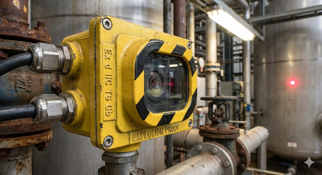
However, successful implementation requires careful consideration. Material compatibility is crucial; different materials absorb laser wavelengths differently. A stainless steel sensor housing may require a fiber laser for a deep annealed mark, while a ceramic sensing element might need a UV laser for a high-contrast surface etch without micro-cracking. Parameter optimization—such as power, speed, frequency, and pulse duration—is key to achieving the desired mark depth, contrast, and speed without causing thermal damage to sensitive internal components.
In conclusion, laser marking is far more than a simple labeling step in sensor production. It is a sophisticated, value-adding process that enhances product reliability, supports stringent regulatory requirements, and enables the smart, connected ecosystems of Industry 4.0. As sensors become more integral and intelligent, the role of permanent, high-quality laser marking in ensuring their performance and traceability will only continue to grow, solidifying its status as an indispensable technology in advanced manufacturing.