In the rapidly evolving landscape of consumer electronics, the integration of sophisticated sensor technology has become paramount. Among these advancements, laser autofocus (LAF) sensors represent a significant leap forward, particularly in the realm of front-facing camera systems for selfies. From an electrical engineering perspective, this technology is not merely a convenience feature but a complex interplay of optics, signal processing, and precision timing.
At its core, a laser autofocus sensor operates on the Time-of-Flight (ToF) principle. A low-power, eye-safe laser diode, typically in the infrared spectrum, emits a modulated light pulse towards the subject. A dedicated sensor, often a single-photon avalanche diode (SPAD) array or a specialized photodiode, detects the reflected signal. The system's microcontroller or dedicated ASIC (Application-Specific Integrated Circuit) then calculates the distance to the subject by measuring the phase shift or the direct time delay between the emitted and received pulses. This process, occurring within milliseconds, provides an absolute distance measurement, unlike traditional contrast-detection autofocus systems that require a "hunting" process.
The electrical design challenges are substantial. Engineers must meticulously manage the laser driver circuit to ensure precise pulse modulation while strictly adhering to laser safety Class I standards. This involves current regulation, thermal management, and often incorporating safety shut-off mechanisms. Concurrently, the receiver circuit demands high sensitivity to detect the faint reflected signal amidst ambient noise. This necessitates transimpedance amplifiers (TIAs) with low noise figures and high gain-bandwidth products, followed by sophisticated filtering and analog-to-digital conversion stages. Signal integrity is critical; even minor interference can skew distance calculations.
For selfie applications, this technology offers transformative benefits. The primary advantage is speed. Laser autofocus achieves focus lock virtually instantaneously, even in challenging low-light conditions where contrast-based systems struggle. This is because the laser system operates independently of ambient light levels, relying on its own active illumination. Furthermore, it enables consistent performance for video calls and rapid-fire self-portraits, eliminating the frustrating focus lag that can blur moments.
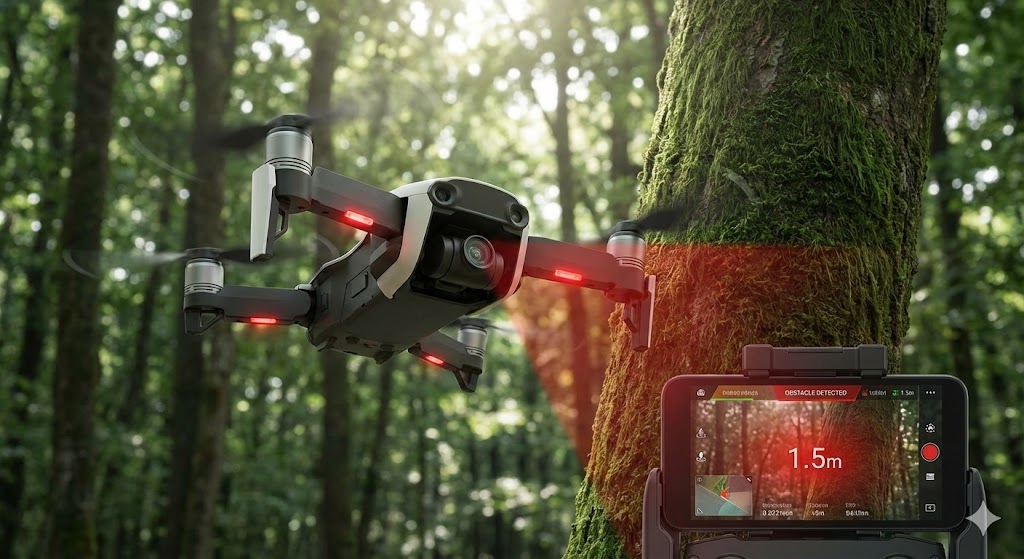
From a system integration standpoint, incorporating a LAF sensor into a smartphone's compact front module requires careful PCB layout and EMI shielding. The sensor, laser diode, and control IC must be positioned to ensure an unobstructed path for the laser beam, often through a small window in the bezel. Power management is another key consideration, as the system must be energy-efficient to avoid draining the battery during frequent use. Modern implementations often use a hybrid approach, where the laser provides an initial rapid distance estimate, which is then refined by the main image sensor's phase-detection or dual-pixel autofocus system for ultimate accuracy.
The implications extend beyond simple selfies. This precise depth-sensing capability is foundational for advanced features like accurate portrait-mode bokeh effects, where the subject is sharply separated from the background based on accurate depth maps. It also enhances augmented reality (AR) experiences in selfie mode by allowing virtual objects to interact more realistically with the user's spatial environment.
Looking forward, the evolution of laser autofocus sensors points towards miniaturization and multi-function integration. We are seeing the development of VCSEL (Vertical-Cavity Surface-Emitting Laser) arrays that are more compact and efficient. Furthermore, the same hardware used for autofocus is often leveraged for proximity sensing and even rudimentary 3D facial mapping, demonstrating the versatile utility of the underlying ToF principle.
In conclusion, the laser autofocus sensor in selfie cameras is a testament to applied electrical engineering. It transforms a user-centric function—taking a clear, quick selfie—into a solved problem through rigorous circuit design, precise component selection, and intelligent system control. As the demand for higher-quality mobile imaging continues, the role of such active sensing technologies will only grow more central, driving further innovation in low-power optoelectronics and high-speed mixed-signal IC design. For engineers, it represents a fascinating field where theoretical principles of light and electricity directly enhance everyday human interaction with technology.