For electrical engineers and technical professionals working with automation, robotics, or precision measurement, understanding the internal architecture of a laser sensor is crucial for optimal application, troubleshooting, and innovation. This detailed teardown analysis provides a component-level examination of a standard time-of-flight (ToF) laser distance sensor, a common and versatile type. The accompanying diagram and description follow industry-standard nomenclature and practices.
External Housing and Interface:
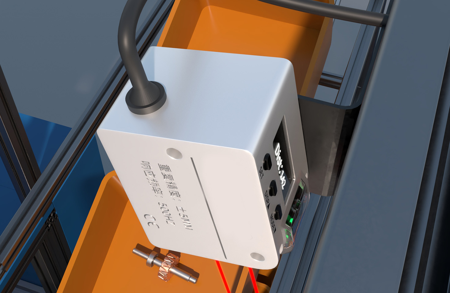
The process begins with the removal of the robust, anodized aluminum housing. This casing serves dual purposes: providing electromagnetic interference (EMI) shielding and acting as a heat sink for internal components. The front features a precision optical-grade glass or polymer window, sealed against dust and moisture ingress (typically rated IP67). The rear panel houses the multi-pin industrial connector (e.g., M12 or M8), which carries power (commonly 12-24V DC), digital communication lines (e.g., IO-Link, RS-232, or analog output), and ground.
Internal Assembly Layout:
Upon opening the housing, the internal PCB assembly is securely mounted on anti-vibration standoffs. The layout is distinctly partitioned into three functional blocks: the optical transmission module, the optical reception module, and the signal processing/control board.

1. Optical Transmission Module:
This module is responsible for generating and projecting the laser beam. Its core is a Class 1 or Class 2 laser diode, operating in the visible red (650nm) or, in more advanced models, infrared spectrum (e.g., 850nm or 905nm). The diode is mounted on a sub-PCB with a dedicated laser driver circuit. This driver provides precise constant current to the diode, ensuring stable optical output power and modulating the beam for the ToF measurement principle. Directly in front of the diode is a collimating lens assembly. This set of micro-lenses shapes the divergent raw laser light into a tight, low-divergence beam, crucial for achieving high spatial resolution and long measurement range.
2. Optical Reception Module:
Positioned adjacent to the transmitter is the receiver path. The returning, reflected laser light first passes through a receiver aperture to limit ambient light noise. It then hits the primary focusing lens, which concentrates the light onto the heart of the receiver: the photodetector. For ToF sensors, this is typically an Avalanche Photodiode (APD) or a Single-Photon Avalanche Diode (SPAD). These specialized semiconductors offer extremely high sensitivity and fast response to detect the faint returning pulse. The APD is housed in a light-tight enclosure to prevent saturation from internal stray reflections or external light.
3. Signal Processing and Control Board:
This is the computational core of the sensor. The faint analog signal from the photodetector is first amplified by a Trans-Impedance Amplifier (TIA). This critical component converts the photodetector's current signal into a usable voltage signal. The amplified signal then feeds into a high-speed Analog-to-Digital Converter (ADC). The digitized signal is processed by the main Digital Signal Processor (DSP) or a powerful microcontroller (MCU) with dedicated hardware accelerators. This processor executes the complex ToF calculation by precisely timing the interval between the emitted laser pulse (a reference signal from the driver) and the detected return pulse. Environmental compensation algorithms for temperature and ambient light are also run here. The board includes voltage regulators for clean power delivery to sensitive analog and digital sections, and the communication interface chip (e.g., for IO-Link or RS-485).
Interconnections and Calibration:
High-frequency coaxial cables or controlled-impedance traces on the PCB connect the laser driver, photodetector, and ADC to preserve signal integrity. A critical, often overlooked component is the temperature sensor (thermistor or IC-based), mounted near the laser diode and optics. Its readings feed into the DSP for real-time wavelength and drift compensation, ensuring long-term stability. During factory assembly, the optical axes of the transmitter and receiver are painstakingly aligned and permanently fixed with epoxy or screws. Each unit undergoes calibration against traceable standards, with correction coefficients stored in a non-volatile EEPROM memory on the main board.
Key Design Considerations Revealed by the Teardown:
* Thermal Management: The direct mounting of the laser driver and diode onto the metal housing is a clear design choice for heat dissipation.
* Signal Integrity: The physical separation of high-power digital sections from low-level analog receiver circuits minimizes noise coupling.
* Robustness: Conformal coating on the PCB is often visible, protecting against humidity and condensation.
* Optical Precision: The quality of the collimating and focusing lenses is paramount; any dust or misalignment here directly impacts performance.
This internal view demystifies the laser sensor, transforming it from a black box into a comprehensible synergy of optics, analog electronics, and digital processing. For engineers, this knowledge informs better system integration, aids in diagnosing failure modes (e.g., a degraded laser diode output or a contaminated optical window), and inspires potential modifications or custom designs for specialized applications. Understanding the teardown diagram is a fundamental step in mastering the application of these critical industrial components.