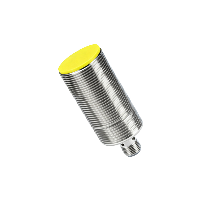
In the rapidly evolving landscape of industrial automation, consumer electronics, and IoT, the relentless drive towards miniaturization has reached a new pinnacle with the development of the world's smallest proximity sensors. These microscopic marvels, some measuring less than 1.0 x 0.5 x 0.3 mm, are not merely a testament to engineering prowess but are fundamentally reshaping design possibilities across countless applications. Their emergence marks a critical inflection point, enabling functionality in spaces previously deemed impossible and pushing the boundaries of what's achievable in smart, compact devices.
The core technology enabling this dramatic size reduction lies in advanced Micro-Electro-Mechanical Systems (MEMS) fabrication and cutting-edge semiconductor packaging. Unlike traditional inductive or capacitive sensors that relied on larger coils or plates, these ultra-miniature sensors often utilize sophisticated photoelectric or specialized RF principles. They are manufactured using processes similar to integrated circuit production, allowing for the precise etching and layering of sensing elements, signal conditioning circuits, and communication interfaces onto a single, minuscule silicon chip. This system-on-chip (SoC) approach eliminates bulky external components, drastically cuts power consumption to the microamp range, and enhances reliability by reducing interconnection points.
The applications for these tiny sentinels are vast and transformative. In the consumer electronics sector, they are indispensable for enabling bezel-less smartphone displays. Nestled invisibly under the screen glass, they accurately detect the presence of a user's ear during a call, instantly turning off the display to prevent accidental touch inputs and save battery life. Similarly, in true wireless stereo (TWS) earbuds, these sensors provide intuitive in-ear detection, automatically pausing playback when an earbud is removed. The robotics and drone industries leverage them for precise obstacle detection in confined spaces, while advanced medical devices, such as endoscopic capsules and implantable monitors, utilize their non-contact sensing capabilities in extremely sensitive environments. Furthermore, they are becoming key enablers in next-generation human-machine interfaces (HMI), allowing for touchless gesture control on wearables and ultra-compact industrial controls.
However, the design and integration of the world's smallest proximity sensors come with significant engineering challenges. The primary trade-off for extreme miniaturization is often a reduced sensing range, typically limited to a few centimeters, which is perfectly adequate for its intended applications but requires meticulous placement. Designers must also contend with heightened sensitivity to environmental optical noise, electrical interference, and precise alignment during assembly. Advanced algorithms for digital filtering and ambient light rejection are integrated directly into the sensor's firmware to ensure stable operation. Thermal management and mechanical robustness are also critical, as the tiny package must withstand reflow soldering temperatures and potential mechanical stress in final products.
Looking ahead, the future of miniaturized sensing is converging with trends in AI and energy harvesting. The next generation of these sensors will likely incorporate edge-processing capabilities, allowing them to make simple contextual decisions locally, further reducing power consumption and system latency. Furthermore, research into self-powered sensors using minute ambient energy (light, vibration, RF) promises truly autonomous, maintenance-free sensor nodes for the Internet of Things. As packaging technologies like wafer-level chip-scale packaging (WLCSP) advance, we can anticipate even smaller form factors with enhanced performance.
In conclusion, the world's smallest proximity sensors represent far more than an incremental improvement; they are a foundational technology enabling a new wave of innovation. By providing reliable, low-power, and non-contact detection in a footprint once considered unattainable, they are unlocking novel product designs and smarter, more responsive automated systems. For engineers and designers, understanding the capabilities, limitations, and integration nuances of these components is no longer a niche skill but an essential competency for developing the next generation of cutting-edge electronic and mechatronic systems. Their continued evolution will silently but powerfully drive progress in making our devices more intuitive, compact, and interconnected.