In the realm of high-reliability electronics manufacturing, particularly for sensors deployed in automotive, aerospace, and medical devices, the integrity of solder joints is paramount. Traditional post-solder cleaning and rework methods, such as mechanical grinding or chemical fluxes, often introduce micro-cracks, residual stress, or contamination. These imperfections can compromise electrical conductivity, mechanical strength, and long-term reliability. Laser ablation, or laser打磨, has emerged as a superior, non-contact technique for the precise refinement and rework of sensor solder joints. This process utilizes focused laser energy to selectively remove excess solder, reshape joint profiles, or eliminate bridging and icicles without affecting the adjacent substrate or components.
The core principle involves the interaction of high-intensity laser pulses with the solder material. Typically, fiber lasers or pulsed Nd:YAG lasers with wavelengths in the near-infrared spectrum (e.g., 1064 nm) are employed. These wavelengths are well-absorbed by common solder alloys like SAC305 (Sn96.5Ag3.0Cu0.5) or lead-based solders, while being highly reflective to many substrate materials like FR-4 or ceramic. The process is governed by precise control over laser parameters: pulse energy, pulse duration, repetition rate, and scan speed. Short pulse durations (nanosecond to picosecond range) are preferred to minimize the heat-affected zone (HAZ). The laser energy rapidly heats, melts, and vaporizes the targeted solder material, with the vapor pressure ejecting the molten droplets. An assist gas, often nitrogen or clean dry air, is co-axially delivered to blow away debris and prevent re-deposition.
The advantages of laser solder joint refinement are multifaceted. First, it offers unparalleled precision and selectivity. The laser spot can be focused down to tens of microns, allowing for the removal of microscopic solder bridges between fine-pitch pins on sensor ICs without risking damage to the delicate package or nearby traces. Second, it is a cold ablation process relative to the substrate. The localized energy input ensures that thermal stress on the temperature-sensitive sensor element (like a MEMS structure or piezoelectric crystal) is negligible, preserving its calibration and performance. Third, it is a dry, chemical-free process. This eliminates the need for solvent cleaning, preventing ionic contamination that could lead to electrochemical migration and sensor drift. Fourth, it enables process automation and consistency. Integrated with vision systems and programmable galvanometer scanners, the laser path can be dynamically adjusted based on real-time inspection, ensuring every joint meets the exact geometric and volumetric specifications.
Key applications in sensor manufacturing include:
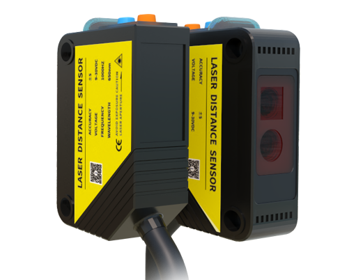
1. De-bridging and Short Removal: Critical for miniaturized sensor arrays where solder paste misprinting can cause electrical shorts between adjacent pads. Laser ablation cleanly severs the unintended connection.
2. Solder Joint Reshaping: For sensors requiring specific joint geometry for optimal mechanical stress distribution or thermal dissipation, lasers can sculpt the solder fillet to a desired shape, improving fatigue life.
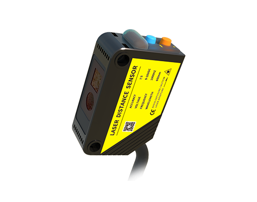
3. Excess Solder Removal: Automated soldering processes like reflow or wave soldering can sometimes deposit excess solder, affecting the sensor's profile or creating parasitic capacitance. Laser ablation reduces the joint to its target volume.
4. Rework and Repair: Instead of desoldering an entire sensor component, localized laser ablation can remove faulty solder for a single pad, allowing for precise component replacement—a vital capability for expensive or long-lead-time sensor modules.

Implementing a laser ablation system requires careful consideration. Material compatibility studies are essential to determine the optimal wavelength and fluence (energy density) threshold for the specific solder alloy without damaging the underlying pad (often copper with a Ni/Au or OSP finish). Process development involves creating a digital twin of the solder joint and simulating the ablation depth per pulse to generate an efficient scan pattern. In-line monitoring, using techniques like coaxial melt pool monitoring or post-process 3D laser scanning, is integrated for closed-loop quality control.
In conclusion, laser ablation represents a transformative step in the post-assembly processing of high-performance sensors. By providing a means to achieve perfect solder joint morphology with sub-millimeter accuracy and zero collateral damage, it directly enhances the electrical performance, mechanical robustness, and long-term field reliability of sensors. As sensor packages continue to shrink and performance demands escalate, laser-based refinement transitions from a specialized rework tool to an essential inline process in the smart factory, ensuring that every connection in a critical sensor is flawless.