In the rapidly evolving landscape of industrial automation, machine vision, and precision measurement, Laser CMOS (Complementary Metal-Oxide-Semiconductor) sensors have emerged as a pivotal technology. These devices integrate the focused energy of laser illumination with the high-speed, low-power imaging capabilities of CMOS sensors, creating powerful tools for non-contact detection, profiling, and analysis. This article delves into the operational principles, key advantages, diverse applications, and future trends of Laser CMOS sensors.
At its core, a Laser CMOS sensor system consists of three fundamental components: a laser source, optics (lenses or diffusers), and a CMOS image sensor. The laser, typically a semiconductor diode laser, emits a coherent, monochromatic light beam. This beam is shaped—often into a line, dot, or structured pattern—by optical elements and projected onto a target object. The CMOS sensor, positioned at a specific angle relative to the laser emitter, captures the reflected or scattered light from the object's surface. Sophisticated onboard or connected processors then analyze the captured image. By applying principles of triangulation, time-of-flight (ToF), or structured light, the system can extract precise geometric data, such as distance, height, thickness, presence, or a complete 3D profile of the object.
The synergy between laser illumination and CMOS technology confers several compelling advantages. First is High Precision and Resolution. The coherent nature of laser light provides a sharp, high-contrast image on the target, which, when captured by modern high-resolution CMOS chips (often with global shutters for capturing fast-moving objects without distortion), allows for micron-level measurement accuracy. Second is Speed and Real-Time Processing. CMOS sensors are inherently suited for high-speed data readout, enabling frame rates in the thousands per second. This is critical for inline inspection in manufacturing where products move rapidly on conveyor belts. Third is Robustness in Challenging Environments. Laser light, being of a specific wavelength, can often overcome ambient lighting interference. Combined with optical filters on the sensor that block all but the laser's wavelength, these systems perform reliably in variable factory lighting conditions. Fourth is Compact Size and Low Power Consumption, hallmarks of CMOS technology, which facilitate integration into portable devices and dense machine designs.
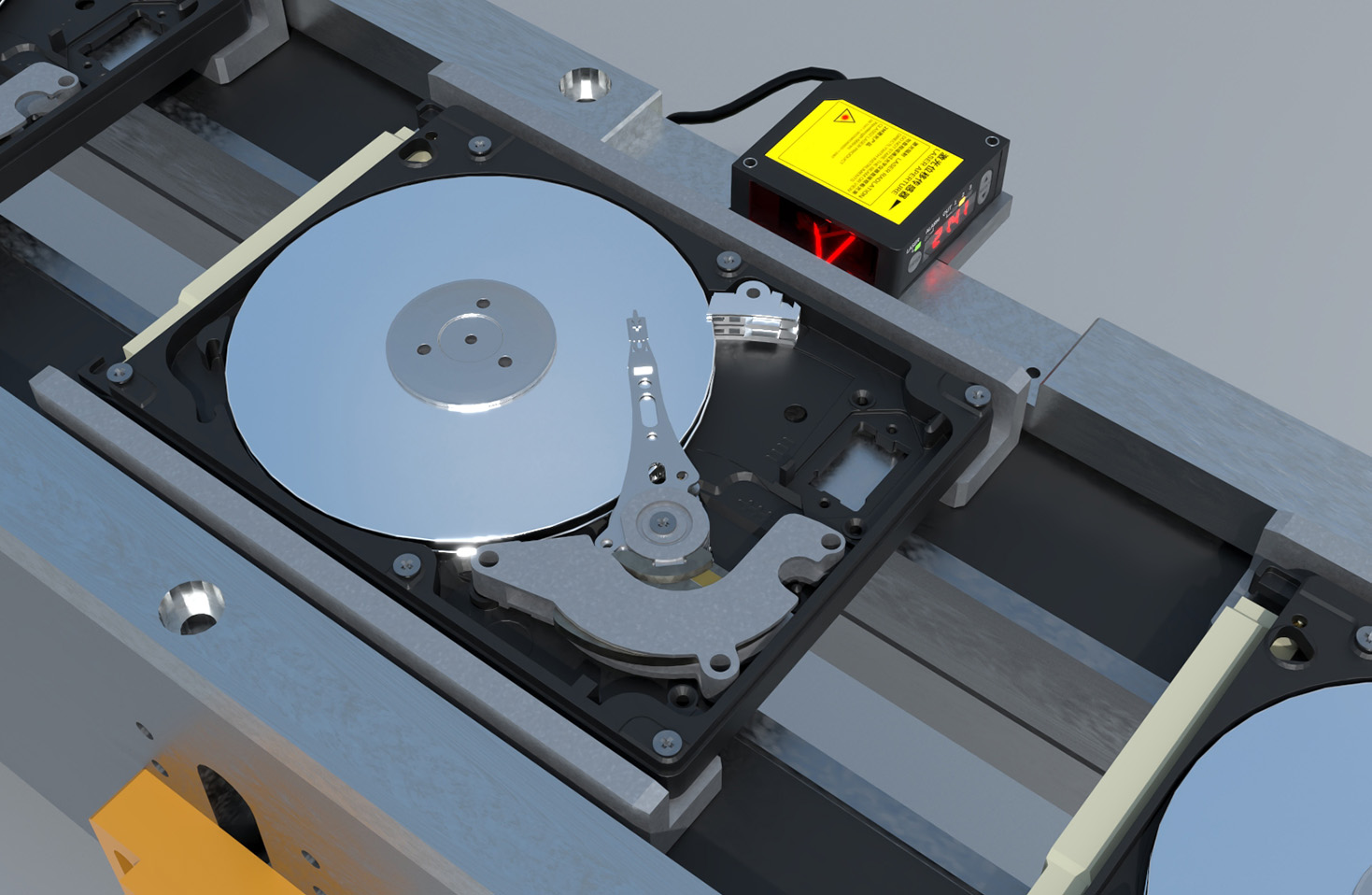
The applications of Laser CMOS sensors span numerous industries, driving efficiency and quality control. In Automotive Manufacturing, they are used for robotic guidance, weld seam inspection, and gap-and-flush measurement on car body panels. The Electronics Industry relies on them for solder paste inspection (SPI), component placement verification, and PCB warpage measurement. Within Logistics and Packaging, these sensors perform vital tasks like box dimensioning, label verification, and parcel sorting. Metrology and Quality Assurance laboratories use high-end versions for reverse engineering, surface defect detection, and precision part alignment. Emerging fields like Agricultural Robotics employ them for crop monitoring and selective harvesting, while Consumer Electronics integrate miniaturized versions for facial recognition and augmented reality features.
Looking ahead, several trends are shaping the future of Laser CMOS sensors. The integration of Artificial Intelligence (AI) and Edge Computing is paramount. Instead of streaming raw data to a central PC, sensors with embedded AI chips can perform real-time defect classification and decision-making at the source, reducing latency and bandwidth. Advancements in SPAD (Single-Photon Avalanche Diode) CMOS sensors are enhancing the capabilities of laser-based Time-of-Flight systems, allowing for longer range and higher accuracy in 3D imaging. There is also a strong push towards Miniaturization and Cost Reduction, making this technology accessible for broader, high-volume applications. Finally, the development of Multi-Spectral and Hyperspectral Laser Imaging combines spectral analysis with spatial data, opening new frontiers in material identification and biological sensing.
In conclusion, Laser CMOS sensors represent a mature yet continuously innovating technology at the intersection of photonics and semiconductor electronics. Their ability to deliver fast, accurate, and reliable dimensional data non-invasively makes them indispensable in modern industrial and scientific contexts. As processing power increases and costs decrease, their adoption will only widen, solidifying their role as a cornerstone of smart automation and precise digital measurement.