In the rapidly evolving landscape of industrial automation and precision measurement, Surface-Mount Device (SMD) laser sensors have emerged as a cornerstone technology. These compact, highly reliable components are integral to modern manufacturing, quality control, and robotics. Unlike their through-hole predecessors, SMD laser sensors are designed for automated PCB assembly, offering superior performance in a minimal footprint. This article delves into the operational principles, key applications, and critical factors for selecting the right SMD laser sensor for your project.
At their core, SMD laser sensors operate on the principle of optical triangulation or time-of-flight measurement. A laser diode emits a focused beam of coherent light onto a target surface. The reflected light is then captured by a photodetector, typically a position-sensitive device (PSD) or a CMOS/CCD array. By analyzing the position or the phase shift of the reflected spot, the sensor's onboard processor can calculate precise measurements of distance, displacement, height, or presence. The SMD packaging ensures these optical and electronic components are hermetically sealed and resistant to vibrations, dust, and minor contaminants, making them ideal for harsh industrial environments.
The applications for SMD laser sensors are vast and varied. In electronics manufacturing, they are indispensable for chip mounting, solder paste inspection, and PCB warp detection. Their high speed and accuracy enable real-time feedback for pick-and-place machines. In automotive assembly lines, these sensors perform critical gap and flush measurements between body panels, ensuring premium build quality. Furthermore, they are pivotal in non-contact thickness gauging of films, foils, and delicate materials, where physical contact could cause damage. The miniaturization trend in consumer electronics has further propelled the demand for ultra-compact SMD laser sensors capable of inspecting microscopic components.
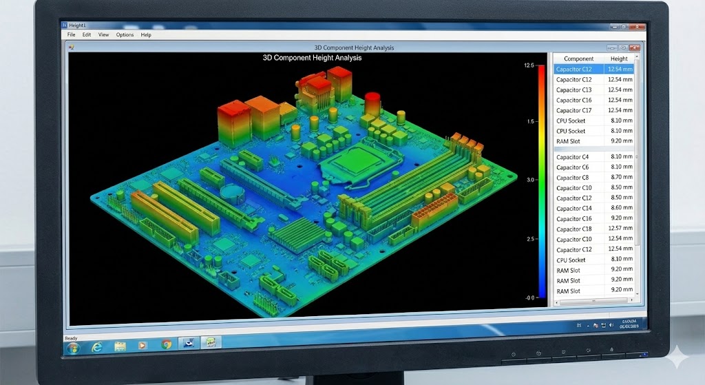
When selecting an SMD laser sensor, several technical parameters demand careful consideration. First, the measurement range and resolution must align with the application's tolerance requirements. A sensor with sub-micron resolution might be necessary for semiconductor inspection, while millimeter-level precision suffices for object detection. Second, the laser's wavelength (commonly 650nm red or 850nm infrared) affects its visibility and performance on different surface materials; red lasers offer a visible spot for easier alignment, while infrared is less distracting in human environments. The response time, or sampling rate, is crucial for high-speed production lines. Environmental robustness, indicated by Ingress Protection (IP) ratings and operating temperature ranges, ensures longevity. Finally, the output interface (digital I/O, analog voltage/current, or serial communication like IO-Link) must be compatible with the existing control system.
Integration of SMD laser sensors into a system requires attention to mounting stability, alignment, and ambient light conditions. Even slight misalignment can lead to significant measurement errors. Many modern sensors come equipped with intelligent features such as background suppression, which filters out light from objects beyond the set range, and teach-in functions for quick parameter setting via a button or software. Regular calibration against a known standard is recommended to maintain long-term accuracy.
Looking ahead, advancements in laser diode technology and signal processing algorithms are pushing the boundaries of what SMD laser sensors can achieve. We are seeing trends towards even smaller form factors, lower power consumption, and enhanced smart capabilities like integrated data analytics and predictive maintenance alerts. As Industry 4.0 and the Internet of Things (IoT) permeate the factory floor, these sensors will increasingly serve as critical data nodes, providing the precise, real-time information necessary for agile and intelligent manufacturing systems.
In conclusion, SMD laser sensors represent a sophisticated fusion of optics, electronics, and packaging technology. Their selection and application require a nuanced understanding of both the sensor's capabilities and the specific demands of the task. By carefully evaluating the technical specifications and environmental factors, engineers can leverage these powerful tools to achieve unprecedented levels of automation, quality, and efficiency in their operations.