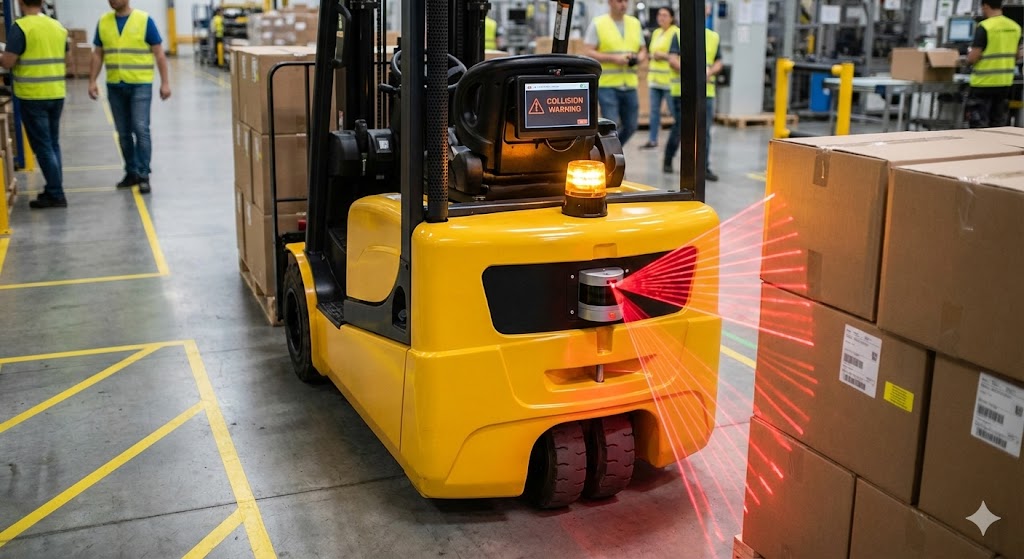
The manufacturing of laser sensors represents a sophisticated intersection of optics, electronics, and precision engineering. These devices, which utilize laser light to detect, measure, or profile objects, are foundational to modern automation, safety systems, and scientific instrumentation. The production process is a meticulous journey from raw materials to calibrated, application-ready units, demanding stringent controls at every stage.
The journey begins with the core component: the laser diode or emitter. Fabrication of these semiconductor light sources occurs in cleanroom environments, using epitaxial growth techniques like Metal-Organic Chemical Vapor Deposition (MOCVD) to build precise crystalline layers on wafer substrates. This process defines the laser's wavelength, power, and operational characteristics. Following growth, wafers undergo photolithography and etching to define individual emitter structures before being diced into chips. These bare laser dies are then mounted onto submounts or headers, a critical step for thermal management, as excessive heat drastically reduces laser efficiency and lifespan. Wire bonding creates electrical connections, and the assembly is often hermetically sealed within a TO-can or similar package to protect the sensitive semiconductor from environmental contaminants.
Parallel to this, the photodetector or receiver component is manufactured. For many sensors, this involves silicon or InGaAs photodiodes, produced through analogous semiconductor processes. The detector's sensitivity, response time, and spectral range must be carefully matched to the emitter's output. In advanced sensors like LiDAR or time-of-flight units, the detector may be a specialized array, such as a CMOS or CCD sensor, manufactured in dedicated semiconductor foundries.
The heart of sensor assembly is the optomechanical design. Here, the packaged laser and detector are integrated into a housing alongside optical elements. Lenses, fabricated from glass or specialized plastics through grinding, polishing, and coating, are aligned to collimate the emitted laser beam into a tight, focused spot and to collect reflected light efficiently onto the detector. This alignment, often performed with micron-level precision using active alignment systems where the laser is powered during adjustment, is paramount for sensor performance. Misalignment leads to reduced signal strength, inaccurate measurements, and poor signal-to-noise ratios. The housing itself, typically machined from aluminum or engineered polymers, provides mechanical stability, protects internal components, and may include features for heat sinking and environmental sealing (e.g., IP ratings).
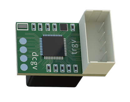
Electronics integration follows. A printed circuit board (PCB) hosts the drive circuitry for the laser, which requires constant current sources to maintain stable optical output, and the amplification circuitry for the weak electrical signal from the photodetector. This often involves transimpedance amplifiers to convert the photocurrent into a usable voltage. Microcontrollers or application-specific integrated circuits (ASICs) are added to manage timing, signal processing, communication protocols (like IO-Link, Ethernet/IP, or analog outputs), and onboard diagnostics. For safety-rated sensors, such as those used in perimeter guarding, redundant circuits and fail-safe designs are implemented and certified to standards like IEC 61496.
Calibration and testing form the final, critical gate before a sensor leaves the factory. Each unit is subjected to a battery of tests in controlled conditions. Key parameters verified include measurement accuracy, repeatability, response time, temperature drift, and long-term stability. Sensors are often cycled through temperature chambers to ensure performance across their specified operating range. Laser output power is meticulously checked to ensure it complies with international laser safety classifications (IEC 60825-1), guaranteeing eye safety for the end-user. This data is frequently logged to the sensor's memory, providing traceability and allowing for compensation algorithms to run during operation.
The applications dictating manufacturing nuances are vast. A simple diffuse-reflective sensor for object detection on a conveyor might prioritize cost-effective, high-volume assembly. In contrast, manufacturing a coherent LiDAR sensor for autonomous vehicles involves complex integration of scanning mirrors (MEMS or mechanical), precise beam shaping optics, and high-speed data processing units. Similarly, laser triangulation sensors for micron-level displacement measurement require exceptionally stable optical benches and calibrated reference standards during production.
Emerging trends continue to reshape manufacturing floors. The integration of advanced materials, like gallium nitride (GaN) for shorter wavelength blue lasers, opens new sensing possibilities. Miniaturization, driven by MEMS technology, allows for incredibly small sensor footprints. Furthermore, the industry is moving towards greater digitization and connectivity, with sensors featuring built-in IIoT capabilities, which necessitates embedding more sophisticated firmware and wireless modules during the final assembly stages.
In essence, laser sensor manufacturing is not a single process but a cascade of highly specialized disciplines. It requires a deep understanding of semiconductor physics, optical science, electronic design, and mechanical engineering. The relentless drive for higher precision, greater reliability, smaller size, and lower cost pushes manufacturing technologies forward, enabling these critical components to become the invisible eyes of an increasingly automated and data-driven world.