In the realm of industrial automation, consumer electronics, and automotive systems, proximity sensors play a pivotal role. Understanding their internal composition is crucial for engineers, technicians, and enthusiasts alike. High-quality component images serve as invaluable educational and diagnostic tools, revealing the intricate architecture that enables non-contact detection. This article delves into the visual breakdown of common proximity sensor types, explaining what each component image reveals about function and design.
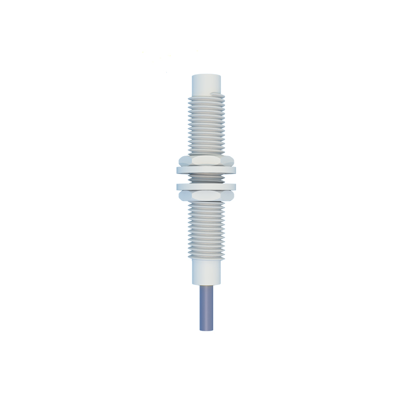
A standard inductive proximity sensor, designed to detect metallic objects, reveals a distinct internal layout when viewed in cross-sectional component images. The front face typically houses a protective sensing face, often made of a ferrite material or plastic, which shields the internal coil. Behind this, the core component—a coiled copper wire wound around a ferrite core—is clearly visible. This coil is part of an oscillator circuit. Component images often show this coil connected to a small printed circuit board (PCB) housing the oscillator, demodulator, and output switching circuitry. The housing, usually metallic (like nickel-plated brass or stainless steel) or polymer, provides electromagnetic shielding and mechanical robustness. A set of wires or a connector exits from the rear, carrying power and the output signal. These images highlight the sensor's simplicity and durability, with no moving parts.
Capacitive proximity sensors, capable of detecting both metallic and non-metallic materials, share a similar external form but differ internally. Component images of these sensors prominently feature a sensing electrode, often a metal plate or ring, positioned behind the front dielectric material (the sensing face). This electrode forms one plate of a capacitor. The images clearly show this electrode connected to an oscillator circuit on the PCB, which is more sensitive than its inductive counterpart. The circuitry is tuned to detect changes in capacitance caused by an object entering the electrostatic field. The housing must prevent false triggering, so images often emphasize the shielding arrangement that isolates the active sensing area. The presence of a sensitivity adjustment potentiometer on the PCB is a common detail visible in high-resolution component photos.
Photoelectric sensors, another major proximity detection family, have a markedly different internal structure as shown in component images. For a through-beam type, the transmitter and receiver are separate units. Component images of the transmitter show an LED (often infrared) or laser diode, a lens to collimate the light beam, and a driving circuit. The receiver unit's images reveal a phototransistor or photodiode, a matching lens, and amplification/comparison circuitry. In reflective or diffuse models, both emitter and receiver are housed in a single unit. These component images beautifully illustrate the precise alignment of the optical elements on a small PCB, often showing a light barrier or labyrinth to prevent internal optical crosstalk. The housing has a clear window made of glass or specialized plastic.
Ultrasonic proximity sensors present a fascinating internal view. Key components visible in images include the piezoelectric transducer, which acts as both speaker and microphone. It appears as a metallic disc. A damping material (like foam) is often seen behind it to control resonance. The heart is a sophisticated PCB containing a microcontroller that generates high-frequency pulses, listens for echoes, and calculates time-of-flight. Component images may also show a protective mesh or cone that acoustically couples the transducer to the environment while offering physical protection.
Analyzing these component images provides functional insights. For instance, the size and winding density of the coil in an inductive sensor indicate its sensing range and frequency. The quality of the potting compound (a resin filling visible in images) speaks to the sensor's environmental resilience against moisture, vibration, and chemicals. The type of output transistor (PNP or NPN) can sometimes be identified on the PCB, clarifying wiring requirements. Marks on ICs can hint at the specific processing algorithms used, especially in smart sensors.
These images are essential for troubleshooting. A burnt component on the PCB, a cracked ferrite core, or a damaged optical lens—all identifiable through detailed component imagery—can explain sensor failure. For designers, such images inform decisions about housing design, component placement for optimal performance, and thermal management.
In conclusion, proximity sensor component images are more than just technical photographs. They are visual narratives that decode the principles of non-contact sensing. From the coiled wire of an inductive sensor to the precise optics of a photoelectric device, each image tells a story of engineering designed to bridge the physical and electronic worlds. Access to clear, high-resolution component imagery remains a fundamental resource for innovation, maintenance, and effective application of these ubiquitous devices across countless industries.