Introduction
Photoelectric sensors have become a cornerstone of modern smartwatch technology, enabling critical health monitoring and user interaction features. From an electrical engineering perspective, these sensors operate by converting light signals into electrical data, leveraging principles of photometry and semiconductor physics. This article explores the technical design, challenges, and optimization strategies for integrating photoelectric sensors into wearable devices, focusing on power efficiency, signal accuracy, and miniaturization.
Sensor Architecture and Principle
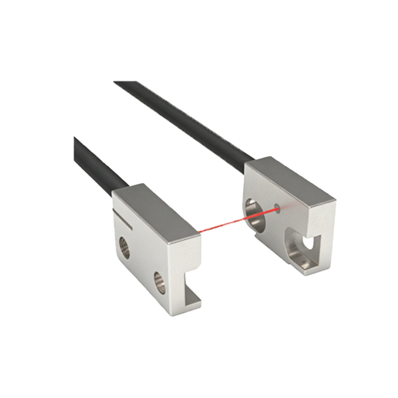
The core of a smartwatch photoelectric sensor typically consists of a light-emitting diode (LED) and a photodetector, such as a photodiode or phototransistor. The LED emits light at specific wavelengths—often green (530 nm) for heart rate monitoring or infrared (940 nm) for proximity detection. Light penetrates the skin and reflects off blood vessels or tissue, with the photodetector capturing the reflected intensity. The output signal, measured as a photocurrent, is then processed using transimpedance amplifiers and analog-to-digital converters. Engineers must optimize the LED driver circuit to balance intensity and power consumption, as continuous operation can drain the battery rapidly.
Signal Processing and Noise Reduction
Raw photoplethysmography (PPG) signals from these sensors are susceptible to motion artifacts, ambient light interference, and low signal-to-noise ratios. To address this, engineers employ digital filtering techniques, such as bandpass filters (0.5–5 Hz) to isolate the heart rate signal from low-frequency motion noise. Adaptive noise cancellation using accelerometer data is a common practice, where the motion signal is subtracted from the PPG signal. Additionally, high-dynamic-range photodetectors with automatic gain control help maintain signal integrity under varying skin tones and environmental lighting conditions.
Power Management Strategies
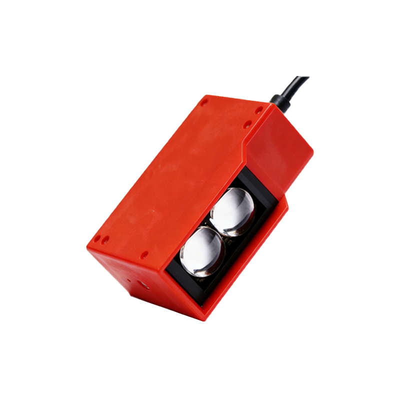
Power efficiency is a paramount concern in wearable devices. Photoelectric sensors often operate in pulsed mode rather than continuous illumination, reducing average current consumption. For instance, the LED may be driven with short pulses (e.g., 10–20 ms) at a duty cycle below 1%, while the photodetector is synchronized to sample only during these pulses. Engineers also integrate low-dropout regulators (LDOs) to stabilize the supply voltage and minimize quiescent current. Advanced sleep modes, such as deep sleep with wake-on-interrupt, further extend battery life during periods of inactivity.
Miniaturization and Packaging
The physical integration of photoelectric sensors into a smartwatch requires careful consideration of optical isolation and thermal management. To prevent crosstalk between the LED and photodetector, engineers design opaque barriers or use optical epoxy with high refractive index. The sensor package must be hermetically sealed to protect against sweat and moisture, while maintaining a low profile (typically<1 mm). Surface-mount technology (SMT) and chip-scale packaging (CSP) allow for compact layouts, but thermal dissipation from the LED must be managed through heat spreaders or via arrays.
Clinical Accuracy and Calibration
For health-monitoring applications, photoelectric sensors must meet clinical standards for accuracy. Calibration involves testing against reference instruments, such as electrocardiograms (ECGs) for heart rate, and adjusting the LED wavelength and intensity for different skin tones (e.g., Fitzpatrick scale types I-VI). Engineers also implement adaptive algorithms that learn user-specific baseline signals, improving accuracy during exercise or low-perfusion states. Compliance with regulations like the FDA’s Class II medical device requirements often dictates the design validation process.
Future Trends and Challenges
Emerging trends in photoelectric sensor technology for smartwatches include multispectral sensing (e.g., red, green, and IR LEDs) for blood oxygen saturation (SpO2) and lactate monitoring. However, challenges remain in reducing power consumption for continuous monitoring and improving signal quality under high-motion conditions. Innovations in silicon photomultipliers (SiPMs) and flexible photodetectors promise enhanced sensitivity and form factor. As an electrical engineer, the focus must remain on system-level optimization, balancing performance, cost, and user experience.
Conclusion
Photoelectric sensors in smartwatches represent a sophisticated intersection of optics, electronics, and software. By mastering circuit design, signal processing, and power management, engineers can deliver reliable, accurate, and efficient health-monitoring features. Continued research into new materials and integration techniques will drive the next generation of wearable technology, further blurring the line between consumer electronics and medical devices.