1. Introduction to Photoelectric Sensor Structure
Photoelectric sensors are critical components in industrial automation, converting light signals into electrical outputs for object detection, distance measurement, and presence sensing. The structural diagram of a typical photoelectric sensor includes three primary sections: the emitter, the receiver, and the signal processing unit. The emitter often uses an LED or laser diode to generate a modulated light beam, which is directed through an optical lens system to ensure collimation and focus. The receiver, typically a photodiode or phototransistor, captures the reflected or interrupted light. The signal processing unit amplifies, filters, and converts the analog signal into a digital output (e.g., NPN or PNP transistor switch). Understanding the layout of these components is essential for troubleshooting and application design, as physical alignment and environmental factors like dust or ambient light can affect performance.
2. Emitter Section: Light Source and Optics
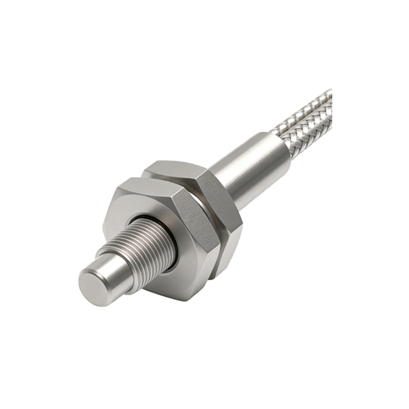
The emitter section is the core of the sensor's light generation. It consists of a light source, usually an infrared LED (e.g., 850 nm or 940 nm wavelength) or a visible red laser (650 nm) for long-range applications. The light source is driven by a constant current circuit to maintain stable intensity. A collimating lens is placed in front of the LED to shape the beam into a narrow, parallel ray for through-beam sensors, or a diverging beam for diffuse reflective sensors. For background suppression sensors, an additional prism or lens array may be used to create a precise focal point. The mechanical housing protects the emitter from shock and vibration, using materials like stainless steel or polyamide to meet IP67 or higher ingress protection ratings.
3. Receiver Section: Photodetector and Filtering
The receiver section is designed to detect the incoming light signal with high sensitivity. A photodiode (e.g., PIN photodiode) is typically used due to its fast response time (nanoseconds) and low noise. The photodiode is reverse-biased to create a depletion region that generates a photocurrent proportional to light intensity. An optical band-pass filter is often mounted in front of the photodiode to block ambient light (e.g., sunlight or fluorescent flicker) and only pass the sensor's specific wavelength. For polarized retro-reflective sensors, a polarizing filter is added to distinguish the emitted light from reflections from shiny objects. The photocurrent is then converted to a voltage via a transimpedance amplifier (TIA), ready for processing.
4. Signal Processing Unit: Amplification and Comparator
The signal processing unit is the brain of the photoelectric sensor. It includes a high-gain operational amplifier (op-amp) to boost the weak photovoltage from the TIA. A band-pass filter (e.g., 1 kHz to 10 kHz) is applied to reduce electrical noise from the power supply or nearby motors. The filtered signal enters a comparator circuit, which compares it against a reference threshold voltage. If the signal exceeds the threshold (indicating an object is present), the comparator triggers a logic output. Some advanced sensors incorporate a microcontroller for adjustable hysteresis, sensitivity, or timing functions (e.g., on-delay or off-delay). The output stage uses a transistor (e.g., NPN or PNP) to drive an external load, typically a PLC input or relay.
5. Mechanical Housing and Environmental Protection
The structural diagram also includes the mechanical housing, which is crucial for sensor durability. Common housing shapes include cylindrical (M12, M18) or rectangular (30x30 mm) designs. The housing is sealed with O-rings and potted with epoxy resin to achieve IP67 or IP69K ratings for washdown environments. The lens is often made of polycarbonate or glass, with an anti-reflective coating to minimize light loss. Wiring connections are typically via a 4-pin M12 connector or pre-wired cable. For harsh industrial conditions, metal sleeves and silicone seals protect against temperature extremes (-25°C to +60°C). Proper grounding and shielding are integrated to prevent electromagnetic interference (EMI) from affecting sensor performance.
6. Conclusion and Application Insights
In summary, the structural diagram of a photoelectric sensor reveals a sophisticated interplay of optics, electronics, and mechanics. By breaking down the emitter, receiver, signal processing, and housing, engineers can better select and install sensors for applications like conveyor belt object detection, packaging line counting, or automated guided vehicle (AGV) navigation. For optimal performance, always consider the sensor's response time (e.g.,<1 ms), operating distance (e.g., 0.1 m to 30 m), and environmental factors like fog or dust. Regular maintenance, such as cleaning the lens and checking alignment, ensures long-term reliability. Refer to the manufacturer's datasheet for detailed structural diagrams and electrical specifications for your specific model.