Introduction to Photoelectric Sensor Evolution
The field of photoelectric sensors has undergone significant transformation over the past decade, driven by demands for higher precision, faster response times, and robust integration in industrial automation. As a senior electrical engineer, I have observed how innovations in semiconductor materials and signal processing are reshaping these devices. Modern photoelectric sensors now leverage infrared, laser, and ambient light rejection technologies to operate reliably in harsh environments, from dusty factory floors to high-vibration assembly lines.
Core R&D Focus: Enhanced Detection and Miniaturization
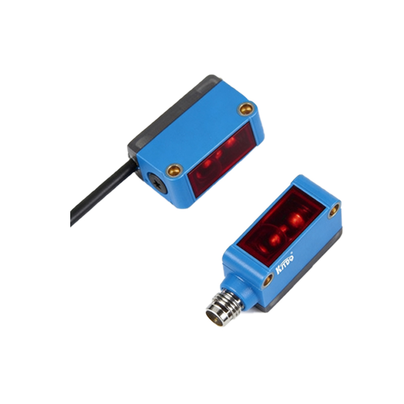
Current research and development efforts prioritize two key areas: improving detection range and sensor miniaturization. By utilizing advanced photodiodes with higher sensitivity and low-noise amplifiers, engineers have achieved detection distances exceeding 50 meters for through-beam sensors. Simultaneously, new packaging techniques, such as surface-mount technology and system-in-package designs, have reduced sensor footprints by up to 40% without compromising performance. This miniaturization enables integration into compact robotic grippers and conveyor systems.
Emerging Technologies: Digital Signal Processing and IoT Readiness
A breakthrough in recent years is the integration of digital signal processing (DSP) chips directly into photoelectric sensors. These DSPs filter out background noise and compensate for temperature drift, ensuring stable output even under fluctuating lighting conditions. Furthermore, IoT-ready sensors now feature embedded communication protocols like IO-Link and EtherCAT, allowing real-time data transmission to PLCs and cloud-based monitoring systems. This connectivity facilitates predictive maintenance and reduces downtime in smart factories.
Challenges in Material Science and Environmental Durability
Despite progress, material selection remains a critical challenge. Photoelectric sensors exposed to chemical vapors or extreme temperatures require specialized housings, such as stainless steel or polycarbonate with UV stabilization. Our R&D team has recently tested new anti-reflective coatings for optical lenses, which minimize signal loss in high-humidity environments. Additionally, ongoing work on nanowire-based photodetectors promises higher quantum efficiency and lower power consumption.
Future Trends: Machine Learning Integration and 3D Sensing
Looking ahead, the convergence of photoelectric sensors with machine learning algorithms is poised to revolutionize object recognition. By training neural networks on sensor output data, systems can distinguish between transparent, reflective, or irregularly shaped objects with over 99% accuracy. Another frontier is 3D time-of-flight sensing, where modulated light pulses measure distance and volume, enabling advanced applications in bin picking and autonomous vehicle navigation.
Conclusion: Strategic Implications for Industrial Automation
For electrical industry professionals, staying abreast of these developments is crucial. The next generation of photoelectric sensors will not only replace traditional electromechanical switches but also serve as intelligent nodes in the Industrial Internet of Things. Engineers should prioritize modular designs and open architecture platforms to ensure scalability. As we continue to push boundaries, collaboration between optical physicists and circuit designers will be key to unlocking new capabilities.