Introduction to Photoelectric Sensors in Industrial Automation
Photoelectric sensors are critical components in modern industrial automation, enabling non-contact detection of objects through light emission and reception. The manufacturing process involves precision engineering and strict quality control to ensure reliability in harsh environments. This article outlines the step-by-step fabrication workflow, from raw material selection to final testing.
Raw Material Preparation and Semiconductor Wafer Processing
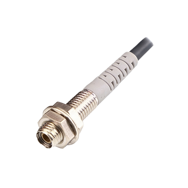
The core of a photoelectric sensor is its optoelectronic semiconductor chip, typically made from silicon or gallium arsenide. The process begins with wafer cleaning and doping to create p-n junctions. Photolithography defines the light-sensitive areas, followed by etching to form photodiodes or phototransistors. After dicing, each die is inspected under a microscope for defects.
Optical Component Assembly: Lenses and Filters
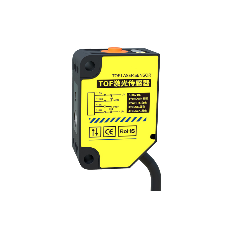
High-precision plastic or glass lenses are molded and coated with anti-reflective layers to optimize light transmission. Bandpass filters are added to block ambient light interference. These components are aligned using automated pick-and-place machines with sub-micron accuracy, then bonded using UV-curable adhesives.
Electronic Circuit Integration and PCB Assembly
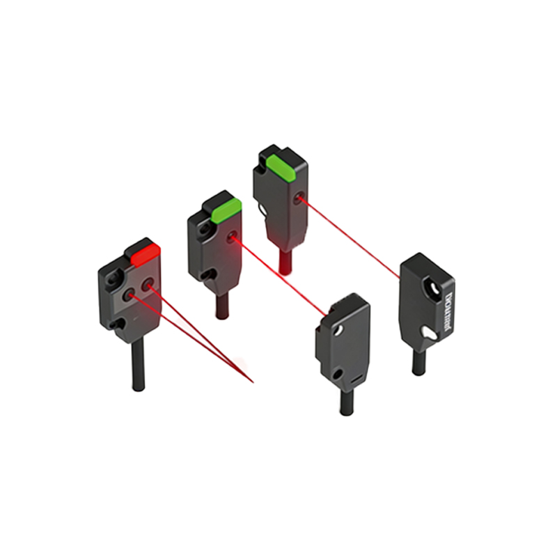
The sensor die is mounted onto a printed circuit board (PCB) via wire bonding or flip-chip technology. Supporting components such as amplifiers, comparators, and output transistors are soldered using reflow ovens. ESD protection circuits are integrated to prevent damage during operation. The PCB is then cleaned and inspected for solder joint quality.
Housing Encapsulation and Sealing
To withstand dust, moisture, and vibration, the assembled PCB is inserted into a metal or plastic housing. Potting compounds like epoxy are injected to encapsulate sensitive electronics, providing IP67 or higher ingress protection. Gaskets and O-rings are installed for sealed cable entries.
Calibration and Sensitivity Adjustment
Each sensor undergoes a calibration process using a reference target and controlled light sources. Engineers adjust the threshold voltage to achieve consistent detection distances. Parameters like response time and hysteresis are fine-tuned via potentiometers or digital interfaces.
Environmental Stress Testing and Quality Assurance
Sensors are subjected to temperature cycling from -40°C to 85°C, humidity exposure at 95% RH, and mechanical shock tests. Output signals are monitored for drift. Only units passing all tests proceed to final packaging.
Final Assembly and Packaging for Distribution
After passing QA, sensors are labeled with serial numbers and specifications. They are packaged in anti-static bags with desiccants and shipped in protective foam-lined boxes. Traceability data is logged in the ERP system for future warranty claims.
Conclusion: Ensuring Reliability in Industrial Applications
The photoelectric sensor manufacturing process demands interdisciplinary expertise in optics, electronics, and materials science. By following this rigorous workflow, engineers deliver sensors that provide consistent performance in factory automation, logistics, and safety systems. Continuous improvement in production techniques further enhances sensor longevity and accuracy.