Introduction to Photoelectric Sensor Receiver Circuits
Photoelectric sensors are widely used in industrial automation for object detection, distance measurement, and motion control. The receiver circuit, as the core component of these sensors, must effectively convert weak reflected or transmitted light signals into stable electrical outputs. This article focuses on the design principles, component selection, and performance optimization of dedicated photoelectric sensor receiver circuits, targeting engineers and technicians in the electrical and automation industries.
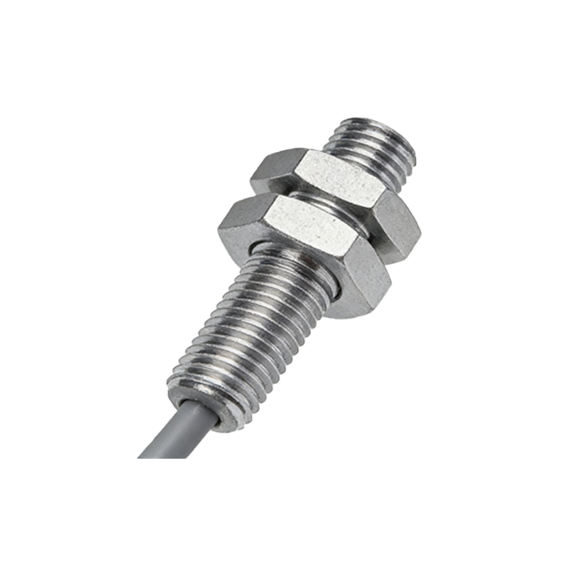
Key Components and Their Functions
A typical photoelectric sensor receiver circuit includes a photodiode or phototransistor as the light-to-current converter, followed by a transimpedance amplifier (TIA) for current-to-voltage conversion. For high-speed applications, a PIN photodiode paired with a low-noise operational amplifier (e.g., OPA series) is recommended. Additional components like bandpass filters and comparators (e.g., LM393) assist in noise rejection and signal thresholding. Ensure power supply decoupling capacitors (0.1 µF and 10 µF) are placed close to IC pins to minimize high-frequency interference.
Circuit Topology and Signal Processing
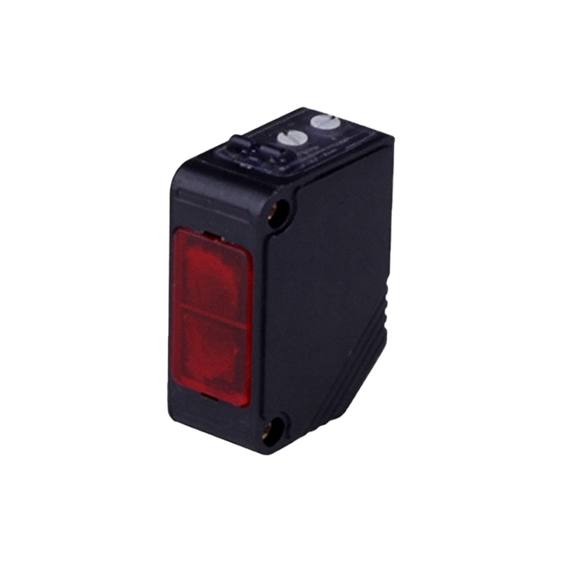
The receiver circuit typically employs a transimpedance amplifier configuration. For example, using an OPA320 with a feedback resistor of 1 MΩ and a capacitor of 1 pF provides a bandwidth of 1 MHz, suitable for most industrial sensors. After amplification, a second-order active low-pass filter (cutoff at 10 kHz) removes ambient light noise. For digital output, a hysteresis comparator with adjustable thresholds (using a potentiometer) ensures clean switching at logic levels (0-5 V for TTL or 0-24 V for industrial PLCs).
Noise Reduction and Environmental Robustness
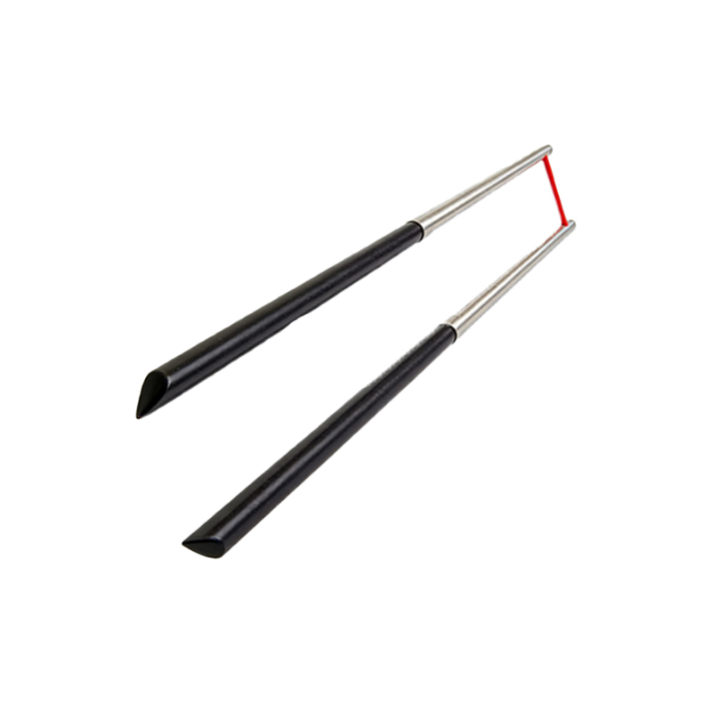
To operate reliably in EMI-prone environments, shield the receiver circuit with a grounded metal enclosure. Use differential signaling (e.g., RS-422) for long-distance transmission. Implement automatic gain control (AGC) via a variable gain amplifier (e.g., VCA821) to handle varying light intensities from 0.1 lux to 100,000 lux. Additionally, incorporate a phototransistor with a daylight filter (e.g., TEPT5700) to reduce interference from sunlight or artificial lighting.
Power Management and Efficiency
For battery-powered or industrial IoT sensors, optimize power consumption. Use a low-dropout regulator (LDO) like TPS7A05 to provide 3.3 V with 1 µA quiescent current. In sleep mode, disable the TIA and comparator via a MOSFET switch (e.g., Si2302) to reduce total current to under 10 µA. For high-speed applications, balance power and response time by selecting operational amplifiers with a slew rate of 10 V/µs or higher.
Testing and Calibration Procedures
After assembly, test the receiver circuit with a calibrated light source (e.g., 850 nm LED at 10 mW/cm²). Measure the output voltage at the TIA stage: expect 1-5 V for typical signals. Adjust the comparator threshold to 50% of the peak amplitude for optimal noise margin. Use an oscilloscope to verify rise time (< 1 µs) and fall time (< 2 µs). For field calibration, employ a microcontroller to auto-tune the gain via an ADC (e.g., ADS1115) and a DAC (e.g., MCP4725).
Application Examples and Future Trends
In conveyor belt systems, a pair of through-beam sensors with optimized receiver circuits can detect objects as small as 1 mm at speeds up to 10 m/s. For automotive LiDAR, dedicated avalanche photodiode (APD) circuits with 200 V bias supplies achieve 100 m range. Future trends include integrated photonic circuits (PIC) for multi-wavelength sensing and AI-driven adaptive thresholding to reduce false triggers in dynamic environments.