1. Introduction to Photoelectric Sensor Disassembly
As an electrical engineer specializing in industrial automation, I often encounter photoelectric sensors in the field. To understand their reliability and performance, nothing beats a hands-on internal disassembly. This article presents a step-by-step breakdown of a typical through-beam photoelectric sensor, revealing its core components and construction. The images captured during this process highlight the precision engineering behind these ubiquitous devices.
2. External Casing and Initial Inspection
The disassembly begins with the sensor’s rugged metal housing, typically made from stainless steel or die-cast zinc. This enclosure is designed to withstand harsh industrial environments, including vibration, moisture, and dust. Using a precision screwdriver set, I removed the four hex screws securing the front cap. The O-ring seal, visible immediately, is critical for IP67 protection. Note the smooth, corrosion-free surface—a sign of quality manufacturing.
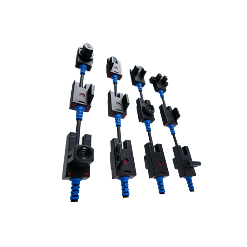
3. Optical Lens and Emitter Assembly
Once the front cap is removed, the optical lens assembly is exposed. This consists of a convex PMMA (polymethyl methacrylate) lens, which focuses the emitted infrared light. Under the lens, the emitter is a high-power GaAs LED soldered onto a ceramic substrate. The lens is held in place by a spring-loaded retainer, ensuring precise alignment. Any misalignment here would directly impact sensing range and accuracy.
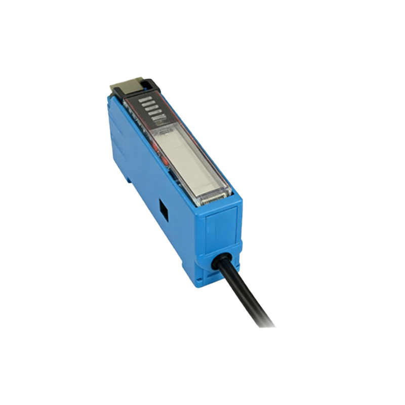
4. Receiver and Photodiode Module
On the opposite side of the PCB, the receiver module features a silicon photodiode with an integrated transimpedance amplifier (TIA). This component converts light intensity into a voltage signal. The photodiode is shielded by a narrow-band optical filter, which blocks ambient light interference, especially from fluorescent or sunlight sources. The gold-plated pins on the module reduce contact resistance and improve signal integrity.
5. Signal Processing PCB and Microcontroller
The heart of the sensor lies in the multi-layer printed circuit board (PCB). Here, a low-power microcontroller (MCU, e.g., STM32 series) handles signal amplification, noise filtering, and output logic. I observed high-quality electrolytic capacitors for power supply decoupling and a voltage regulator for stable 3.3V operation. The PCB traces are routed with care to minimize crosstalk between the analog and digital sections.
6. Output Stage and Protection Circuits
The output stage includes a Darlington transistor pair for NPN/PNP switching, capable of sinking or sourcing up to 100mA. Additionally, TVS diodes and a series resistor provide protection against overvoltage and reverse polarity. These components are often overlooked but are vital for field reliability, especially when the sensor is connected to long cable runs in noisy environments.
7. Cable Gland and Strain Relief
Finally, the cable gland assembly features a brass connector with a rubber grommet for strain relief. Inside, the wires are soldered to the PCB and encapsulated with epoxy to prevent short circuits. The internal wiring uses 22 AWG stranded copper, tinned for corrosion resistance. This robust design ensures the sensor maintains connectivity even under mechanical stress.
8. Conclusion and Key Takeaways
In summary, a photoelectric sensor is a marvel of industrial design, integrating optics, electronics, and mechanical robustness. The disassembly reveals that quality components, precise assembly, and effective shielding are what make these sensors reliable for years of service. For engineers, understanding these internals helps in troubleshooting and selecting the right sensor for specific applications.