Introduction to Photoelectric Sensor Receiver Circuits
Photoelectric sensors are fundamental components in industrial automation, relying on precise receiver circuits to detect light signals and convert them into usable electrical outputs. The receiver circuit is the critical element that determines the sensor's sensitivity, response time, and overall reliability. This article delves into the core principles, common topologies, and key design considerations for effective photoelectric sensor receiver circuits, providing a technical foundation for engineers and designers in the field.
Core Components and Signal Flow
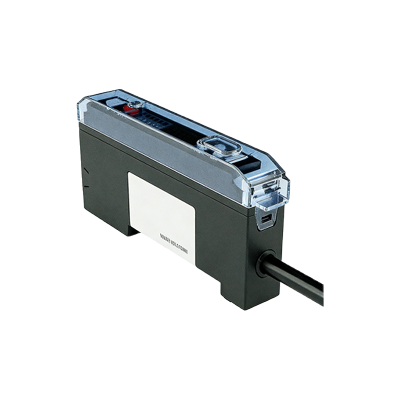
A typical receiver circuit begins with a photodetector, most commonly a phototransistor or photodiode. These components generate a small current proportional to the incident light intensity. This微弱 signal is then fed into a transimpedance amplifier (TIA), which serves as the first and most crucial amplification stage. The TIA converts the photocurrent into a voltage while minimizing noise introduction. Following this, additional signal conditioning stages, such as voltage amplifiers, comparators, and filters, are employed to shape the signal, eliminate ambient light interference, and provide a clean, digital output compatible with control systems like PLCs.
Transimpedance Amplifier Design Considerations
The design of the transimpedance amplifier is paramount. Key parameters include the feedback resistor value, which sets the gain, and the feedback capacitor, essential for stability and bandwidth control. A high-value feedback resistor increases sensitivity but can also increase noise and reduce bandwidth. Designers must carefully select operational amplifiers with low input bias current and low noise to preserve signal integrity. Stability analysis is critical to prevent oscillation, often requiring careful PCB layout with proper grounding and shielding to minimize parasitic capacitance.
Noise Reduction and Ambient Light Rejection
Industrial environments are electrically noisy. Receiver circuits must incorporate strategies to mitigate both electrical noise and interference from ambient light sources. Electrical noise reduction involves using bypass capacitors, choosing low-noise components, and implementing proper shielding. For ambient light rejection, techniques such as modulating the emitted light source (e.g., with a specific frequency) and using a synchronous demodulation circuit in the receiver are highly effective. This allows the circuit to respond only to the modulated signal, effectively filtering out constant or slowly varying ambient light.
Output Stage and Interface Logic
After signal conditioning, the output stage defines how the sensor communicates with external devices. A comparator circuit with hysteresis (Schmitt trigger) is commonly used to convert the analog signal into a crisp digital signal, preventing chatter near the threshold. The output can be configured as NPN (sinking) or PNP (sourcing) transistor logic, or as a push-pull configuration, to interface with a wide range of PLC inputs or other control circuitry. Protection components like flyback diodes for inductive loads and current-limiting resistors are essential in this stage for long-term reliability.
Practical Layout and Testing Guidelines
A theoretically sound design can fail due to poor implementation. PCB layout for photoelectric receiver circuits requires meticulous attention. Keep analog signal paths short, especially around the TIA. Use a solid ground plane and separate analog and digital ground sections if necessary. Power supply lines should be well-decoupled. During testing, use an oscilloscope to probe signals at each stage, verifying gain, bandwidth, and the absence of oscillation. Testing under various lighting conditions and with the intended light source is crucial to validate ambient light rejection and overall performance.
Conclusion and Future Trends
Designing a robust photoelectric sensor receiver circuit balances sensitivity, speed, noise immunity, and cost. Mastery of the transimpedance amplifier, intelligent signal processing for noise rejection, and careful physical implementation are the pillars of success. Future trends point toward greater integration, with application-specific integrated circuits (ASICs) combining the photodetector and sophisticated signal processing on a single chip, offering improved performance and reduced design complexity for next-generation sensor systems.