Introduction to Photoelectric Sensor Development
The development cycle of a photoelectric sensor is a meticulous engineering process that transforms a conceptual need into a reliable, market-ready industrial component. This cycle encompasses a series of interdependent phases, from initial specification definition to final production and support. For engineers and project managers in automation, understanding this lifecycle is crucial for planning resources, managing timelines, and ensuring the final product meets stringent performance, durability, and cost targets. Unlike simpler electronic devices, photoelectric sensors must operate flawlessly in diverse and often harsh industrial environments, making their development a complex interplay of optical engineering, electronics, mechanical design, and software firmware development.
Phase 1: Requirement Analysis and Specification
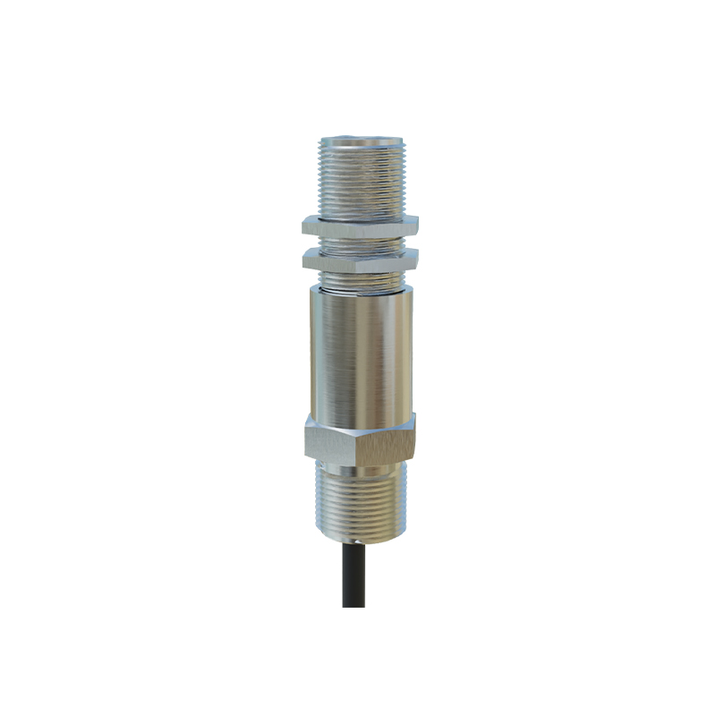
This foundational phase determines the project's trajectory. It involves close collaboration with marketing teams and potential end-users to define the sensor's exact purpose. Key parameters are established, including sensing range (short, medium, or long), detection mode (through-beam, retro-reflective, or diffuse), required output type (digital PNP/NPN, analog, IO-Link), and housing material (typically metal or plastic for specific IP ratings). Environmental specifications are critical: operating temperature range, resistance to chemicals, dust, and water ingress (IP67/IP69K), and immunity to electrical noise. This phase results in a detailed Product Requirements Document (PRD) that serves as the blueprint for all subsequent engineering work.
Phase 2: Optical and Electronic Design
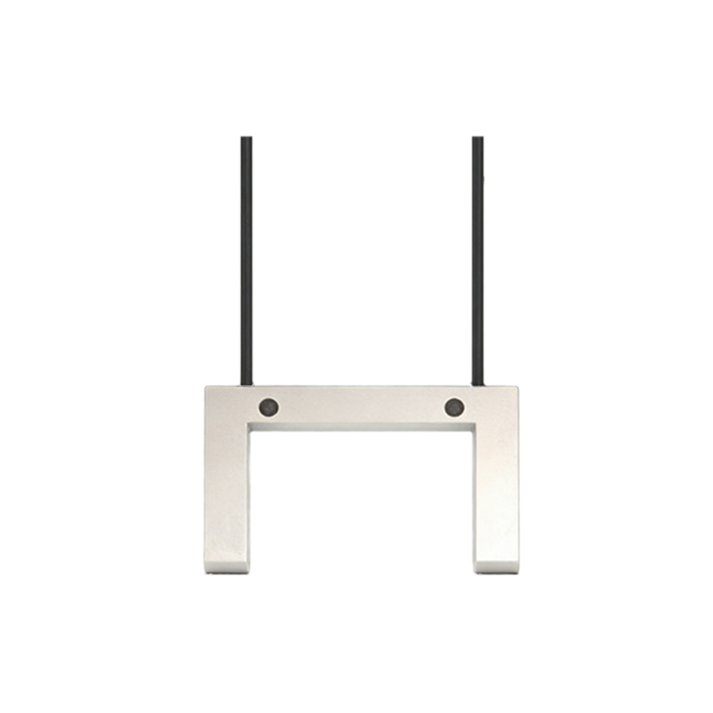
Here, the theoretical specifications become tangible designs. Optical engineers select the appropriate light source (LED, laser) wavelength (visible red, infrared) and lensing system to achieve the desired beam pattern and sensing characteristics. Concurrently, electronic engineers design the circuitry for the transmitter and receiver. This includes the driver circuit for the light emitter, the highly sensitive amplifier circuit for the photodetector (often a phototransistor or photodiode), and signal conditioning logic. Power management, noise filtering, and protection against reverse polarity or short circuits are integral parts of the schematic design. Simulations are run to predict performance under various conditions.
Phase 3: Mechanical Design and Prototyping
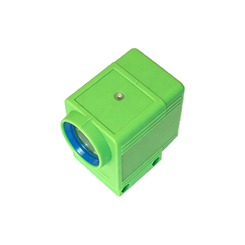
The mechanical design phase focuses on creating a robust housing that protects the delicate internal components. Using CAD software, engineers design the enclosure to meet the IP rating, provide secure mounting options (e.g., M8, M12, M18 threaded barrels or brackets), and allow for precise alignment of the optical windows. Material selection is vital for thermal management, chemical resistance, and EMI shielding. Once the 3D models are finalized, rapid prototyping techniques, such as 3D printing or CNC machining, are used to create functional prototypes. These first physical units allow for initial fit, form, and basic function testing.
Phase 4: Firmware Development and Integration
Modern intelligent photoelectric sensors are powered by embedded microcontrollers. Firmware developers write the code that controls the sensor's logic: modulating the light pulse to enhance noise immunity, implementing teach-in functions for setting sensitivity, managing output signals, and enabling advanced features like background suppression or precise analog value reporting. For sensors with IO-Link capability, firmware must include the complete IO-Link device description. This phase runs parallel to hardware development, with integration testing occurring as soon as the first electronic prototypes are available.
Phase 5: Rigorous Testing and Validation
This is arguably the most critical phase for ensuring reliability. Prototypes undergo exhaustive testing that far exceeds normal operating conditions. Environmental stress tests include thermal cycling, humidity exposure, and vibration/shock tests. Optical performance is validated against the PRD, checking sensing range, repeatability, and response time under different target colors and surfaces. Electrical tests verify EMC compliance, surge immunity, and long-term stability. This phase often reveals design flaws, leading to iterative refinements in the hardware, firmware, or mechanical design before proceeding.
Phase 6: Pre-Production and Certification
Once the design is frozen, a small pre-production batch is manufactured using the intended production tools and processes. This run validates the manufacturing workflow and ensures consistency. Units from this batch are used for final qualification testing and to obtain necessary industry certifications, such as CE, UL, or ATEX for hazardous locations. Documentation, including datasheets, user manuals, and installation guides, is finalized. Supply chain logistics for components are also solidified during this stage.
Phase 7: Mass Production and Launch
With certifications in hand, mass production begins. Automated assembly lines are calibrated for efficiency and quality control. In-line testing, such as functional optical tests and electrical parameter checks, is performed on every single unit. Statistical process control (SPC) monitors production quality. Concurrently, the product is officially launched to the market through distribution channels, supported by marketing campaigns and technical training for sales engineers and distributors.
Phase 8: Post-Launch Support and Iteration
The development cycle does not end at launch. Engineering teams provide ongoing technical support, address field application questions, and monitor field failure rates. Customer feedback is collected and analyzed. This information feeds into the planning for future product iterations or next-generation models, thus restarting the development cycle. Continuous improvement may lead to cost-reduced versions, enhanced feature sets, or variants for new market segments.