The Fundamental Principle of Light to Electricity Conversion
The external photoelectric effect, a cornerstone of modern photoelectric sensing technology, describes the phenomenon where electrons are emitted from a material's surface upon exposure to electromagnetic radiation, typically light. This emission occurs when photons, the fundamental particles of light, possess sufficient energy to overcome the material's work function—the minimum energy required to liberate an electron from its bound state. For engineers, this is not merely a quantum mechanical curiosity but the operational bedrock of vacuum phototubes, photomultiplier tubes (PMTs), and certain specialized photodiodes. The kinetic energy of the emitted photoelectrons is directly proportional to the frequency of the incident light, as famously described by Einstein's photoelectric equation, and is independent of the light's intensity. This direct correlation between photon energy and electron emission enables precise detection and measurement of light across various industrial applications.
Key Components and Material Science
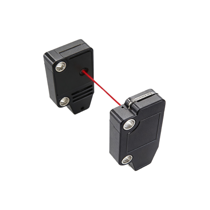
The heart of a sensor leveraging the external photoelectric effect is the photocathode. This is a specially prepared electrode coated with materials possessing a low work function, such as cesium-antimony compounds or bismuth-silver-cesium alloys. The choice of photocathode material is critical as it determines the sensor's spectral response—the range of light wavelengths to which it is sensitive. For instance, a cesium-antimony photocathode exhibits peak sensitivity in the blue and ultraviolet regions. This photocathode is housed within an evacuated glass or metal envelope to prevent electron collisions with gas molecules, ensuring efficient emission and collection. An anode, held at a positive potential relative to the cathode, collects the emitted photoelectrons, generating a measurable photocurrent that is directly proportional to the intensity of the incident light.
Operational Mechanism in Sensor Design
In a practical photoelectric sensor, the process begins with light striking the photocathode. If the photon energy exceeds the work function, photoelectrons are ejected. In a simple phototube, these electrons travel through the vacuum to the anode, creating a circuit current. For applications requiring extreme sensitivity, such as low-light-level detection or particle physics, the photomultiplier tube (PMT) is employed. In a PMT, the initial photoelectrons are accelerated towards a series of electrodes called dynodes. Each electron striking a dynode causes the emission of several secondary electrons through a process called secondary emission. This cascade effect can amplify the initial signal by a factor of millions, producing a large, easily measurable output pulse from even a single photon event. This high gain and fast response time are unparalleled by semiconductor-based sensors.
Advantages for Demanding Industrial Applications
Sensors based on the external photoelectric effect offer distinct advantages in specific industrial and scientific contexts. Their primary benefit is exceptionally high gain and single-photon sensitivity, making them ideal for spectroscopy, medical imaging (like PET scans), and astronomical observations. They exhibit ultra-fast response times, often in the nanosecond or picosecond range, suitable for high-speed laser ranging and fluorescence lifetime measurements. Furthermore, their operation is largely unaffected by temperature variations that can drift the performance of semiconductor sensors. The vacuum enclosure provides excellent isolation from environmental contaminants, ensuring long-term stability and reliability in harsh or controlled environments where consistent performance is non-negotiable.
Limitations and Practical Considerations
Despite their strengths, these sensors present several engineering challenges. They require a stable, high-voltage power supply to operate the anode and dynode chain, which increases system complexity and cost. The vacuum tube construction makes them physically larger, more fragile, and susceptible to damage from excessive light exposure or high current. Their spectral response, while tunable via photocathode material, is generally narrower than that of silicon photodiodes. Over time, the photocathode can degrade, leading to a gradual reduction in sensitivity. Consequently, their use is typically reserved for niche applications where their unique capabilities—extreme sensitivity, speed, and stability—outweigh the drawbacks of size, power requirements, and fragility.
Comparison with Internal Photoelectric Effect Devices
It is crucial to distinguish the external effect from the internal photoelectric effect, which governs common semiconductor sensors like photodiodes, phototransistors, and CCDs. In the internal effect, incident light generates electron-hole pairs *within* the semiconductor bulk, but the charges are not ejected from the material. These internal devices are solid-state, smaller, more robust, operate at lower voltages, and are mass-produced at low cost. They dominate general-purpose industrial automation, consumer electronics, and ambient light sensing. The choice between external and internal effect technologies is thus application-driven: external for ultimate performance in sensitivity and speed; internal for compactness, durability, and economy in high-volume, less extreme sensing tasks.
Future Outlook and Evolving Technology
While semiconductor technology continues to advance, sensors based on the external photoelectric effect maintain their vital role. Ongoing research focuses on developing novel photocathode materials with higher quantum efficiency (more electrons per photon), broader spectral ranges extending further into the infrared, and improved durability. Microfabrication techniques are being explored to create miniaturized, arrayed PMTs or hybrid devices. Furthermore, the integration of advanced readout electronics and digital signal processing is enhancing noise reduction and data acquisition capabilities. For the electrical engineer, understanding this fundamental physical effect remains essential for selecting, designing, or maintaining high-performance sensing systems in scientific research, medical diagnostics, and specialized industrial monitoring where detecting the faintest or fastest light signals is paramount.