Introduction to Ultra-Thin Photoelectric Sensor Chips
Ultra-thin photoelectric sensor chips represent a significant advancement in sensing technology, offering compact designs and high sensitivity for various industrial applications. These chips utilize light-based detection principles to convert optical signals into electrical outputs, enabling precise measurement and control. With thicknesses often below 1 millimeter, they integrate seamlessly into space-constrained environments, such as wearable devices, robotics, and automated systems. The development of these chips focuses on enhancing performance while reducing size, driven by innovations in semiconductor materials and microfabrication techniques. As demand for miniaturized electronics grows, ultra-thin photoelectric sensor chips are becoming essential components in modern engineering solutions, providing reliable and efficient sensing capabilities.
Key Features and Specifications
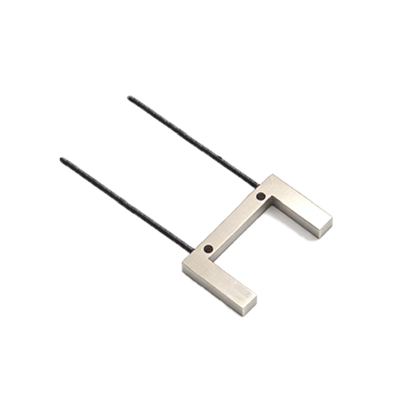
Ultra-thin photoelectric sensor chips are characterized by their slim profiles, typically ranging from 0.5 to 0.8 millimeters, which allow for flexible installation in tight spaces. They offer high sensitivity to light wavelengths, often covering visible and infrared spectra, with response times as fast as microseconds. Key specifications include low power consumption, making them suitable for battery-operated devices, and robust signal-to-noise ratios that ensure accurate detection even in challenging conditions. Many models incorporate advanced features like ambient light rejection and temperature compensation, enhancing their reliability across diverse operating environments. These chips are designed with durable materials, such as silicon or gallium arsenide, to withstand mechanical stress and environmental factors, ensuring long-term stability in industrial settings.
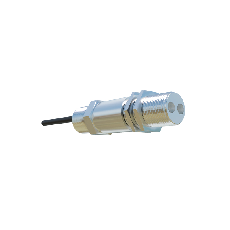
Popular Models and Their Applications
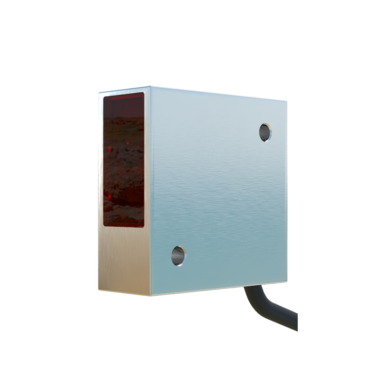
Several leading models dominate the market, each tailored for specific use cases. For instance, the PS-1000 series is renowned for its ultra-thin design of 0.6 millimeters and high precision in proximity sensing, commonly used in smartphones and touchscreens. The LS-2000 model excels in ambient light detection, with a thickness of 0.7 millimeters, ideal for automotive dashboards and smart lighting systems. In industrial automation, the IR-3000 chip, at 0.8 millimeters thick, provides reliable infrared sensing for robotics and safety barriers. These models are engineered to meet stringent industry standards, such as ISO and IEC certifications, ensuring compatibility with global electronic systems. Their versatility extends to medical devices, where they enable non-invasive monitoring, and consumer electronics, enhancing user interfaces with responsive touch controls.
Technological Innovations and Manufacturing
The production of ultra-thin photoelectric sensor chips involves cutting-edge technologies like photolithography and thin-film deposition, which allow for precise layering of semiconductor materials. Innovations in nanotechnology have enabled further miniaturization, improving chip efficiency and reducing costs. Manufacturers focus on optimizing fabrication processes to enhance yield rates and maintain consistency in performance. Recent advancements include the integration of AI algorithms for smart sensing, allowing chips to adapt to dynamic environments and provide real-time data analysis. Quality control measures, such as automated optical inspection and environmental testing, ensure that each chip meets high reliability standards before deployment in critical applications.
Benefits for Industrial and Consumer Use
Ultra-thin photoelectric sensor chips offer numerous advantages, including space savings and enhanced design flexibility, which are crucial for compact electronic products. Their high sensitivity and fast response times improve system accuracy, leading to better performance in automation and control tasks. In consumer electronics, these chips enable sleek, lightweight designs without compromising functionality, contributing to improved user experiences. For industrial applications, they reduce maintenance needs and increase operational efficiency by providing dependable sensing in harsh conditions. Additionally, their low energy consumption supports sustainability goals, aligning with global trends toward eco-friendly technology solutions.
Future Trends and Market Outlook
The future of ultra-thin photoelectric sensor chips looks promising, with ongoing research focused on expanding their capabilities and reducing costs. Emerging trends include the development of flexible and stretchable chips for wearable technology, as well as enhanced integration with IoT networks for smart city applications. Market growth is driven by increasing adoption in sectors like healthcare, automotive, and aerospace, where precision sensing is critical. Analysts predict a steady rise in demand, with innovations in materials science and digitalization fueling further advancements. As technology evolves, these chips are expected to play a pivotal role in enabling next-generation electronic devices and automated systems worldwide.