Introduction to Fingerprint Photoelectric Sensors
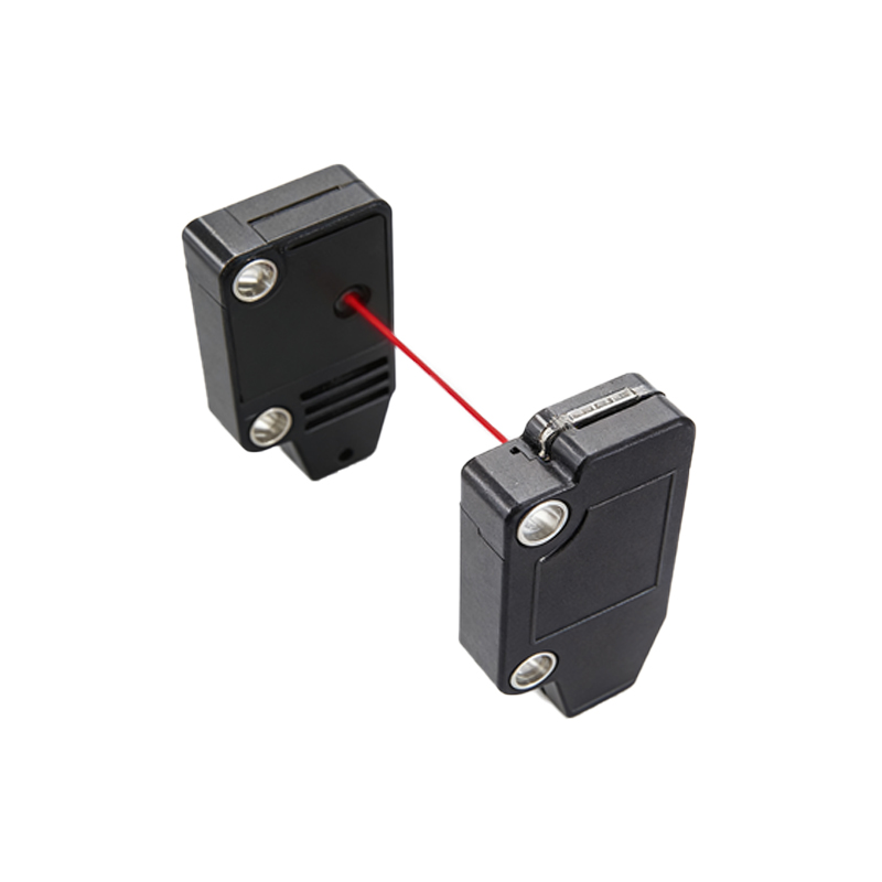
Fingerprint photoelectric sensors represent a pivotal technology in biometric security, fundamentally transforming authentication processes across various industries. These devices operate by capturing the unique ridge and valley patterns of a fingerprint using light-based detection methods. Unlike capacitive sensors that measure electrical conductivity, photoelectric sensors utilize light, typically from LEDs or laser diodes, to illuminate the fingertip. A specialized image sensor, such as a CCD or CMOS array, then captures the reflected light pattern, creating a high-contrast digital image of the fingerprint. This optical capture method is renowned for its durability and resistance to environmental factors like static electricity, making it a preferred choice for high-traffic access control points, time-attendance systems, and secure facility entry. The core principle hinges on the differential reflection of light: ridges, which are in contact with the sensor surface, appear dark, while valleys, which are not in contact, appear bright, resulting in a clear, detailed fingerprint map ready for algorithmic processing.
Operational Principles and Key Components
The functionality of a fingerprint photoelectric sensor is governed by a sophisticated interplay of optical and electronic components. The process initiates with a light source, often a red or green LED array, which projects light onto the fingerprint surface at a specific angle. This angled illumination is crucial for enhancing the contrast between ridges and valleys. The reflected light passes through a series of lenses or a prism system designed to focus the image onto the surface of the photodiode array. This sensor array converts the light intensity at each point into a corresponding electrical signal, pixel by pixel. An analog-to-digital converter (ADC) then digitizes this signal, creating a raw grayscale image. Advanced sensors incorporate total internal reflection (TIR) principles within a prism; when a finger is placed, ridges disrupt the TIR, scattering light, while valleys allow it to reflect internally, thereby generating the distinctive fingerprint image. Signal processing units immediately work to reduce noise, enhance edges, and normalize the image for optimal feature extraction.
Advantages Over Alternative Sensing Technologies
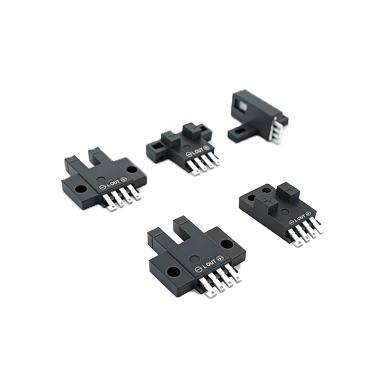
Fingerprint photoelectric sensors offer distinct advantages that solidify their position in the market. Their primary benefit is exceptional image quality and resolution, capable of capturing fine details necessary for reliable 1:1 verification and 1:N identification. They are inherently resistant to electrostatic discharge (ESD), a common failure point for capacitive sensors, which enhances their longevity and reliability in industrial or dry environments. Furthermore, the sensing surface is typically made of durable materials like hardened glass or coated sapphire, making it highly resistant to scratches, wear, and chemical corrosion. This robustness allows for millions of actuations, ideal for public access systems. They are also less susceptible to performance degradation from dry, wet, or lightly soiled fingers compared to some capacitive counterparts. However, it is important to note that they are generally larger in size and may consume more power than ultra-thin capacitive modules, factors that are continually being addressed through miniaturization and low-power LED designs.
Critical Applications in Security and Access Control
The application spectrum for fingerprint photoelectric sensors is vast and critical. In physical access control, they are the cornerstone of high-security door locks, gate entry systems, and secure cabinet access in data centers, financial institutions, and government facilities. Their ability to handle a large database of users makes them ideal for time and attendance tracking in manufacturing plants and corporate offices, replacing traditional punch cards with fraud-proof biometric logging. In the consumer electronics realm, while capacitive sensors dominate smartphones, photoelectric sensors are frequently employed in standalone biometric locks, safes, and high-end laptops where security is paramount. The law enforcement and civil identification sectors rely on high-resolution photoelectric scanners for capturing forensic-quality prints for national ID programs, voter registration, and border control systems, where accuracy and archival quality are non-negotiable.
Integration Challenges and System Design Considerations
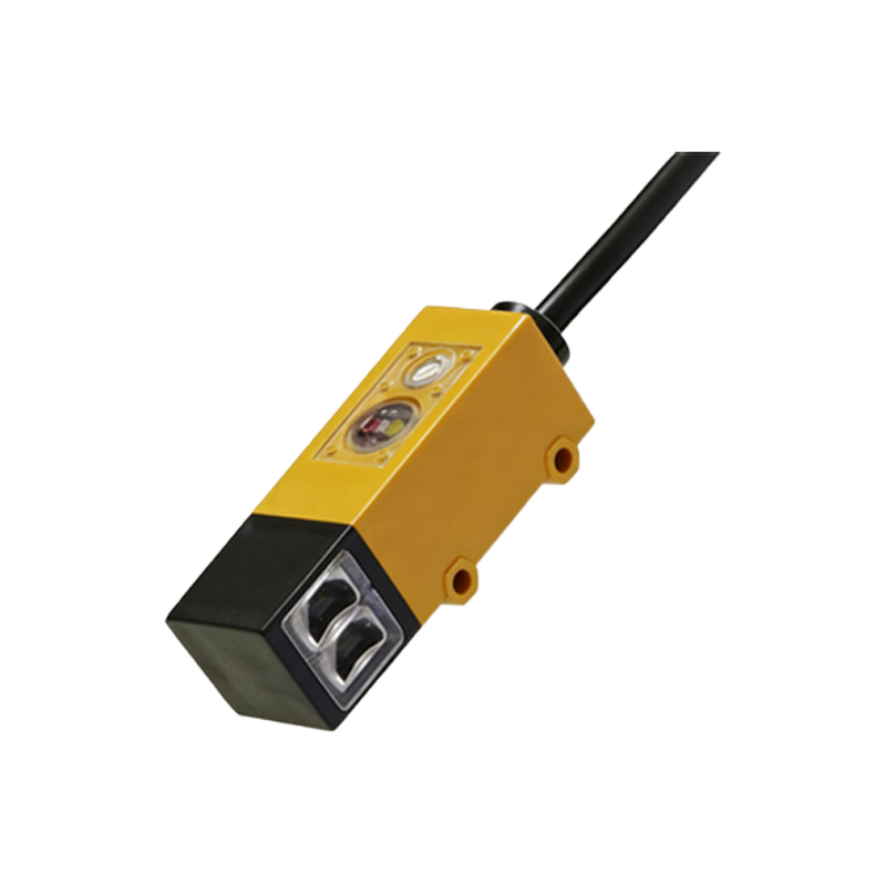
Integrating a photoelectric fingerprint sensor into a complete system requires careful engineering consideration. The optical path must be meticulously designed to prevent ambient light interference, which can degrade image quality. This often necessitates the use of light seals, filters, and controlled illumination. Power management is another key challenge, as the LED light source can be a significant power draw; sophisticated systems use pulsed illumination and sleep modes to conserve energy. The physical form factor and the need for a clean, dry platen surface also dictate industrial design choices, often requiring a bevel or guide to ensure proper finger placement. Furthermore, the system's processing unit must be powerful enough to run complex image preprocessing and matching algorithms in real-time. Engineers must also account for environmental sealing (IP ratings) for outdoor or harsh environment use and ensure the system complies with relevant biometric data protection regulations like GDPR or ISO/IEC 19794 standards.
Future Trends and Technological Evolution
The future of fingerprint photoelectric sensor technology is geared towards higher integration, intelligence, and versatility. A significant trend is the move towards multispectral imaging, which captures fingerprint data from both the surface and subsurface layers of the skin using multiple wavelengths of light. This technology drastically improves performance with dry, wet, or otherwise difficult-to-image fingers. Another direction is the development of ultra-thin, under-display optical sensors for mobile devices, competing directly with ultrasonic and capacitive technologies. The integration of artificial intelligence and machine learning directly at the sensor level (edge AI) is on the horizon, enabling liveness detection to prevent spoofing with fake fingerprints and adaptive image quality enhancement. Furthermore, the convergence with other biometric modalities, such as vein pattern recognition using infrared light, within a single sensor package will create more robust and secure multi-factor authentication solutions for the next generation of security infrastructure.