Introduction to Proximity Magnetic Sensing
Proximity magnetic sensors are fundamental components in modern industrial automation, automotive systems, and consumer electronics. These devices detect the presence or absence of a magnetic field or a ferromagnetic target without physical contact. The core principle relies on the interaction between a sensor element and a magnetic field, which is then translated into an electrical signal. Understanding the schematic of such a sensor is crucial for engineers designing systems for position detection, speed measurement, or limit switching. A typical schematic integrates several key blocks: the sensing element, signal conditioning circuitry, output stage, and often, protection networks. This article delves into the detailed schematic representation, explaining the function of each component and its role in creating a reliable, real-world sensor system.
Core Sensing Element: Hall-Effect and Reed Switches
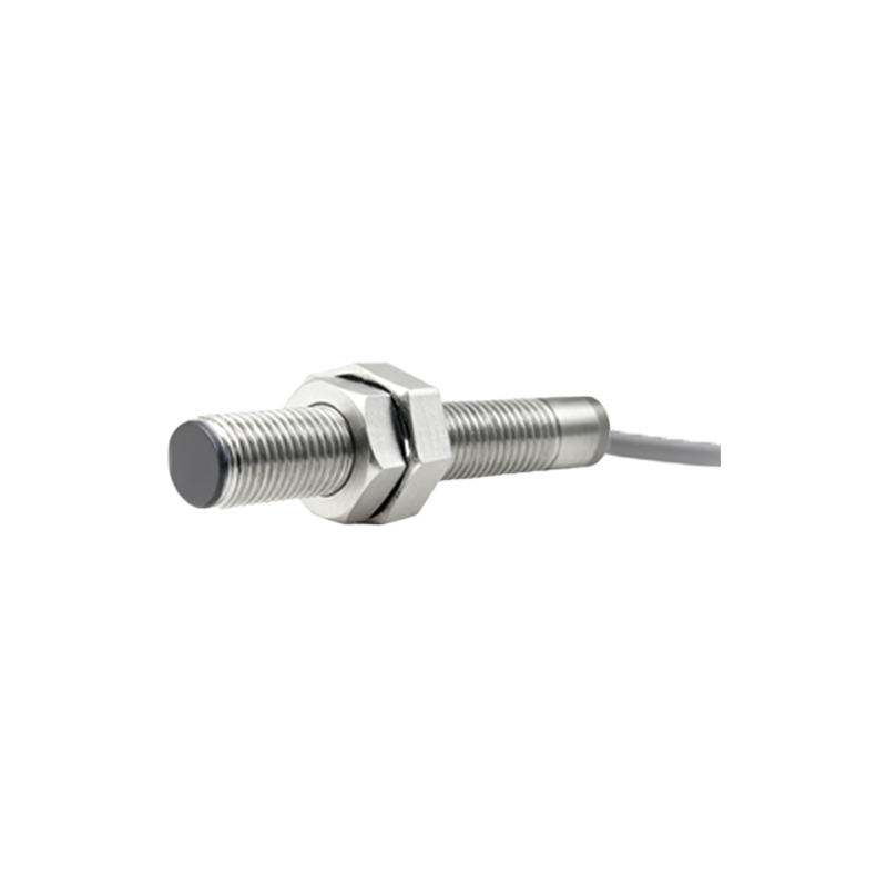
At the heart of the schematic is the sensing element. The two most common types are Hall-effect integrated circuits (ICs) and reed switches. In a Hall-effect based sensor schematic, the symbol for the Hall element is central. It is a four-terminal device: two for supply voltage (Vcc and GND) and two for the differential output signal. When exposed to a magnetic flux density exceeding its threshold, the Hall element generates a millivolt-level potential difference. The reed switch, a simpler passive component, appears in the schematic as a pair of ferromagnetic reeds enclosed in a glass capsule. Its contacts are normally open (NO) or normally closed (NC) and close or open in the presence of a magnetic field, acting directly as a switch in the circuit.
Signal Conditioning and Amplification Stage
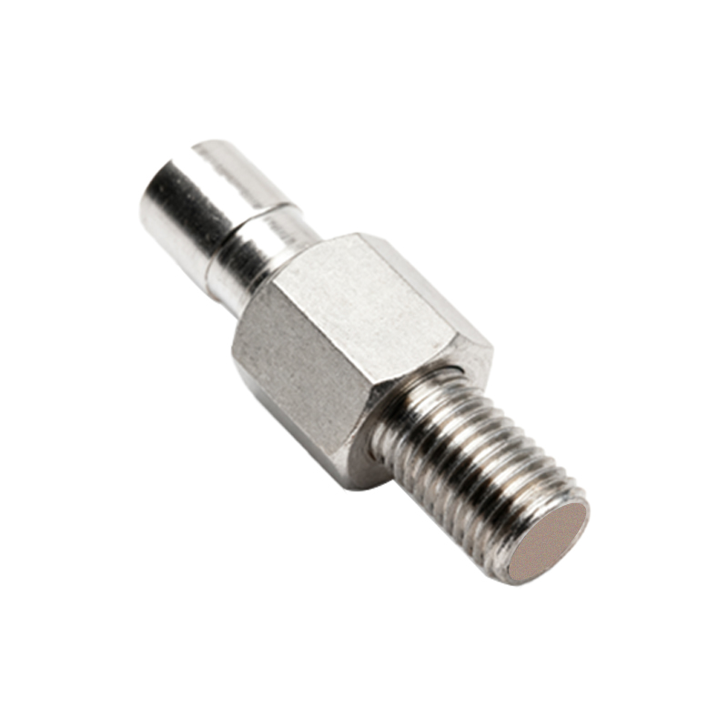
The raw signal from the sensing element is often too weak or noisy for direct use. Therefore, the schematic always includes a signal conditioning block. For Hall-effect sensors, this almost always involves an operational amplifier (op-amp) configured with precise gain resistors. This stage amplifies the small Hall voltage to a robust, usable level. Following amplification, a Schmitt trigger circuit is commonly employed. This component, shown with its distinctive hysteresis symbol, converts the analog amplified signal into a clean, digital output. It provides noise immunity by defining distinct "on" and "off" thresholds, preventing output oscillation when the magnetic field is near the trigger point. This stage is frequently integrated into a single, monolithic Hall-effect IC symbol on the schematic.
Output Configuration and Interface
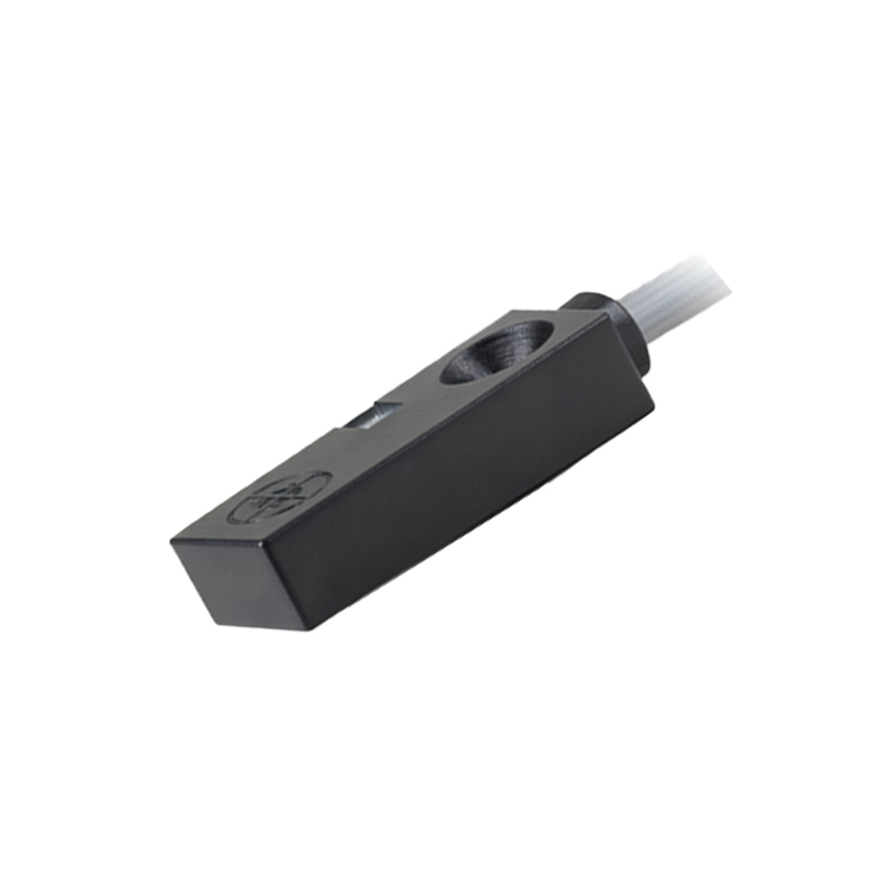
The output stage defines how the sensor communicates with the external controller (e.g., a PLC or microcontroller). Schematics depict this with clear symbols. The three primary output types are: digital open-collector/open-drain, current sink (NPN/PNP), and analog/linear. An open-collector output uses a bipolar junction transistor (BJT) or a MOSFET symbol, with its collector/drain left open. It requires an external pull-up resistor to the logic voltage. NPN (sinking) and PNP (sourcing) transistor symbols show how the sensor switches the load to ground or to Vcc, respectively, crucial for interfacing with different PLC input types. Analog output sensors simply show the output as a voltage pin, whose potential is proportional to the magnetic field strength.
Power Supply and Protection Circuits
A reliable sensor schematic incorporates robust power management and protection. A voltage regulator symbol (like a 78L05) is common if the sensor operates from a wide input range (e.g., 5-24V DC). Decoupling capacitors, placed close to the IC's Vcc pin, are essential for filtering high-frequency noise from the supply line. Protection diodes are critical components. A reverse polarity protection diode is placed in series with the supply input. Transient voltage suppression (TVS) diodes or Zener diodes are often shown across the supply rails to clamp voltage spikes. For the output, a freewheeling or flyback diode symbol is drawn in parallel with an inductive load to protect the output transistor from back-electromotive force (EMF) surges.
Complete Schematic Integration and Layout Considerations
A full proximity magnetic sensor schematic integrates all these blocks into a cohesive system. The drawing follows standard conventions: clear net labels, component designators (R1, C1, U1), and accurate pin assignments for the main sensor IC. For electromagnetic noise immunity in industrial environments, the schematic may note the use of a shielded cable or include an RC filter network on signal lines. While the schematic defines electrical connectivity, accompanying notes often emphasize layout best practices: keeping the sensing element away from noise sources, minimizing loop areas for high-current traces, and ensuring a solid, low-impedance ground plane. This holistic view—from the magnetic field interaction to the clean output signal—is what transforms a theoretical schematic into