Introduction to High-Speed Optoelectronic Sensing
The evolution of sensing technology has been profoundly accelerated by the development of high-speed optoelectronic sensor chips. These sophisticated devices, which seamlessly convert light signals into electrical signals at exceptional speeds, form the backbone of modern data acquisition, communication, and imaging systems. Unlike conventional sensors, their operation hinges on the precise interaction between photons and semiconductor materials within an integrated circuit framework. The core demand driving innovation in this field is the relentless need for higher bandwidth, lower noise, and greater integration, enabling applications from next-generation LiDAR for autonomous vehicles to ultrafast fiber-optic transceivers in data centers. This article delves into the architectural principles, key performance metrics, dominant applications, and the cutting-edge materials shaping the future of these critical components.
Core Architectural Principles and Design
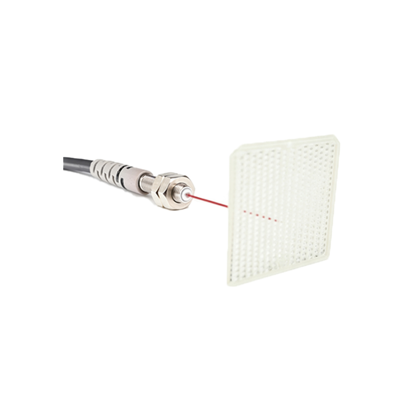
At its heart, a high-speed optoelectronic sensor chip integrates a photodetector region and high-bandwidth electronic circuitry on a single substrate, typically silicon, germanium, or III-V compounds like Indium Phosphide (InP). The photodetector, often a PIN photodiode or an avalanche photodiode (APD), is responsible for the primary photon-to-electron conversion. The design challenge lies in minimizing the carrier transit time and the junction capacitance to achieve high response speed. This photodetector is monolithically or heterogeneously integrated with transimpedance amplifiers (TIAs), limiting amplifiers, and sometimes clock and data recovery (CDR) circuits. The TIA is critical, as it converts the tiny photocurrent into a usable voltage signal with minimal added noise and maximum bandwidth. Advanced designs employ differential signaling, on-chip bias networks, and sophisticated packaging to manage signal integrity, thermal dissipation, and parasitic effects that can degrade high-frequency performance.
Critical Performance Metrics and Trade-offs
Evaluating these chips involves a careful balance of several interdependent parameters. Bandwidth, measured in gigahertz (GHz), defines the maximum data rate the sensor can handle. Responsivity, expressed in amperes per watt (A/W), indicates how efficiently incoming light is converted to electrical current. A higher responsivity is desirable but often conflicts with achieving ultra-high bandwidth. Noise Equivalent Power (NEP) quantifies the minimum detectable optical power for a signal-to-noise ratio of one, defining the system's sensitivity. For APD-based sensors, the gain-bandwidth product is a key figure of merit. Designers constantly navigate trade-offs: increasing bandwidth may reduce responsivity, lowering gain can improve speed, and enhancing sensitivity might require cooling, impacting system size and cost. The pursuit of a higher bandwidth-sensitivity product remains a primary research and development goal.
Dominant Applications in Modern Industry
The application landscape for high-speed optoelectronic sensors is vast and expanding. In telecommunications, they are indispensable in optical fiber receivers for long-haul and metro networks, enabling data rates of 400 Gbps and beyond. LiDAR systems for automotive and robotics rely on these chips to precisely measure time-of-flight for 3D mapping, requiring both high speed and high dynamic range. In scientific instrumentation, time-correlated single-photon counting (TCSPC) modules use ultra-sensitive, fast sensors for fluorescence lifetime microscopy and quantum optics experiments. Furthermore, they are enabling new frontiers in high-speed industrial inspection, optical coherence tomography (OCT) for medical imaging, and free-space optical communication links. Each application imposes unique requirements, pushing chip design toward more specialized and optimized solutions.
Emerging Materials and Integration Techniques
Silicon photonics is a transformative trend, aiming to integrate optical functions like waveguides, modulators, and germanium-based photodetectors directly onto standard silicon CMOS wafers. This promises unprecedented scale, cost reduction, and integration density for datacom applications. Beyond silicon, materials like silicon-germanium (SiGe) alloys offer a favorable balance of speed and compatibility with CMOS processes. For the most demanding performance, especially in the near-infrared spectrum, III-V semiconductors (e.g., InGaAs/InP) are unmatched but face challenges in cost and integration with silicon electronics. Heterogeneous integration techniques, where III-V devices are bonded onto silicon substrates, are becoming a pragmatic pathway to combine the best of both worlds. Research into 2D materials like graphene for photodetection also continues, promising ultra-broadband and ultrafast response.
Future Outlook and Concluding Remarks
The trajectory for high-speed optoelectronic sensor chips points toward higher levels of co-integration, intelligence, and functional diversity. The convergence with silicon photonics will likely yield fully integrated optical "system-on-a-chip" solutions for sensing and communication. There is a growing emphasis on developing sensors for new wavelength ranges, such as short-wave infrared (SWIR), for applications in surveillance and material analysis. Furthermore, the integration of on-chip signal processing, leveraging advanced CMOS nodes, will enable smarter sensors that pre-process data at the source, reducing system latency and power consumption. As the demand for data and precision sensing grows across every sector of technology, the innovation cycle for these critical optoelectronic components will continue to accelerate, enabling capabilities that are currently at the frontier of imagination.