Introduction to Sensing Principles
Proximity and displacement sensors form the backbone of modern industrial automation, providing critical data for position detection, measurement, and control without physical contact. At their core, these devices convert a physical parameter—distance—into a usable electrical signal. The schematic representation of any such sensor is not merely a circuit diagram; it is a blueprint that reveals its operational philosophy, performance boundaries, and integration requirements. Understanding these schematics is paramount for selecting the right sensor, troubleshooting system issues, and designing robust interfaces with controllers like PLCs or embedded systems. This article delves into the schematic intricacies of the most prevalent types: inductive, capacitive, and ultrasonic sensors.
Inductive Proximity Sensor Schematics
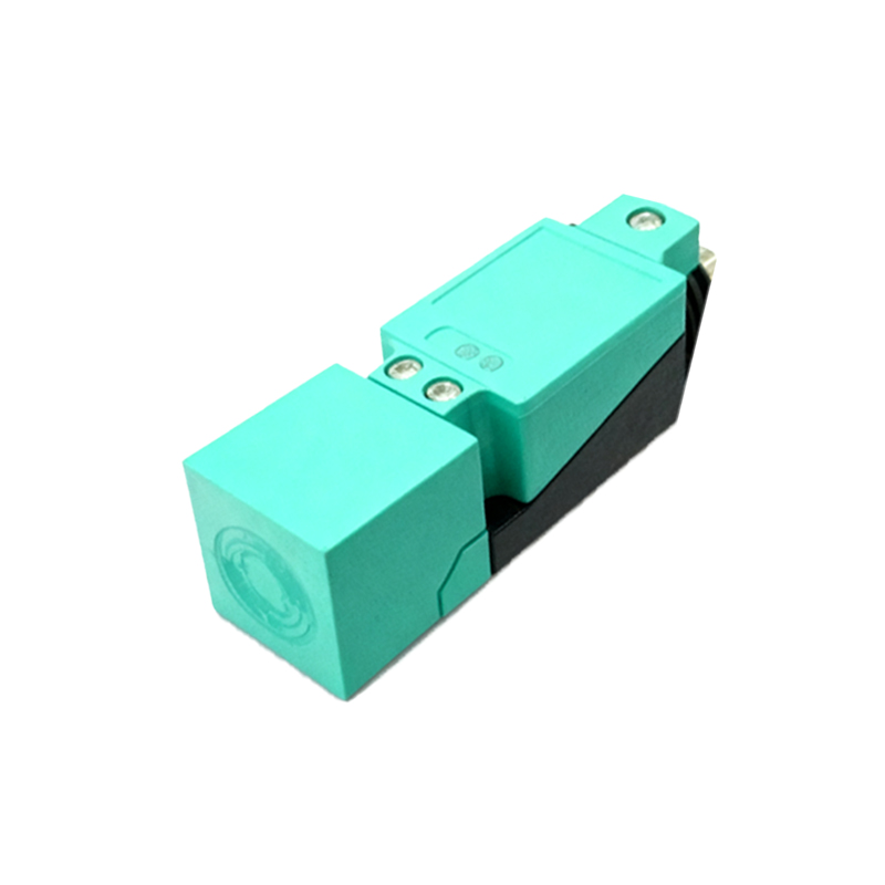
The schematic of a standard inductive proximity sensor reveals a tuned oscillator circuit at its heart. A coil (L), forming the sensor's active face, is part of an LC tank circuit connected to an oscillator (often a Colpitts or Hartley configuration). In the absence of a metallic target, the oscillator runs at its resonant frequency, producing a stable high-frequency electromagnetic field. This signal is fed into a threshold detection stage, typically a comparator or a Schmitt trigger, which keeps the output switch (a transistor, often open-collector NPN or PNP) in its idle state. When a ferrous or non-ferrous metal object enters the sensing field, eddy currents are induced in the target. This represents a power loss, loading the oscillator and causing its amplitude to dampen or cease. The detection circuit senses this drop, triggers the comparator, and switches the output transistor, changing the state of the load connected to the output terminals (OUT, +V, 0V). Protection components like diodes for reverse polarity, RC snubbers for switching transients, and LEDs for status indication are standard features in a complete schematic.
Capacitive Sensor Circuit Analysis
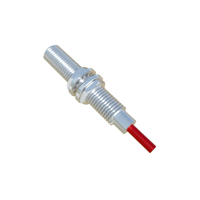
Capacitive sensors, capable of detecting both metallic and non-metallic materials, employ a different schematic approach. The core principle involves measuring a change in capacitance. The sensor face acts as one plate of a capacitor, with the target object acting as the other, and the intervening space as the dielectric. The schematic commonly features an RC or relaxation oscillator circuit where this variable sensing capacitance (Cs) is part of the timing network. As a target approaches, Cs increases, altering the oscillator's frequency or duty cycle. This change is then converted into a DC voltage via a frequency-to-voltage converter (FVC) or is processed by a dedicated capacitive-to-digital converter (CDC) IC. The processed signal is compared against a preset threshold (adjustable via a potentiometer in the schematic labeled "Sens") to drive the output switching stage. Key schematic elements include guard rings or driven shields—auxiliary electrodes connected to a buffer—to focus the sensing field and minimize false triggers from moisture or contamination, a critical consideration in their design.
Ultrasonic Displacement Sensor Block Diagrams
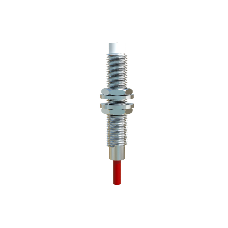
While not a schematic in the pure component-level sense, the functional block diagram of an ultrasonic sensor is essential for understanding its signal flow. The core consists of a piezoelectric transducer, a transmitter circuit, a receiver circuit, and sophisticated timing logic. The transmitter block contains a pulse generator that excites the transducer with a burst of high-frequency electrical pulses (e.g., 40 kHz), converting them into ultrasonic sound waves. The receiver block is highly sensitive, featuring a multi-stage amplifier (often with automatic gain control, AGC) and a filter to amplify the weak returning echo while rejecting noise. The critical timing logic, often implemented with a microcontroller or a dedicated time-to-digital converter (TDC), measures the time-of-flight (ToF) between the transmitted pulse and the received echo. This ToF value, proportional to distance, is then scaled and presented via an analog output (e.g., 4-20 mA, 0-10 V) or a digital communication interface (IO-Link, RS-485) shown in the output stage of the diagram. Synchronization and blanking circuits are crucial to prevent the receiver from being overloaded by the direct transmission pulse.
Output Stage and Interface Considerations
Regardless of the sensing technology, the output stage schematic is vital for integration. The two primary types are discrete (switching) and analog. A discrete output schematic centers on a solid-state switch (MOSFET or bipolar transistor) or an electromechanical relay. Protection is key, featuring freewheeling diodes for inductive loads (DC) or RC snubbers/varistors for AC loads to suppress voltage spikes. Analog output schematics are more complex, involving a digital-to-analog converter (DAC) to produce a voltage or current