In the high-precision world of modern electronics manufacturing, Surface Mount Technology (SMT) laser displacement sensors have become indispensable tools. These non-contact measurement devices provide critical data for process control, quality assurance, and automation, enabling the production of increasingly miniaturized and complex electronic assemblies. This article delves into the operational principles, key application areas, and essential factors for selecting the right sensor for specific SMT tasks.
At their core, SMT laser displacement sensors operate on the principle of optical triangulation. The sensor projects a focused laser beam onto the target surface—be it a component lead, solder paste, or PCB substrate. The reflected light is then captured by a receiving lens at a specific angle and focused onto a position-sensitive detector, typically a CCD or CMOS array. Any change in the target's distance causes a proportional shift in the position of the light spot on the detector. By precisely calculating this shift, the sensor determines the displacement or height with remarkable accuracy, often down to the sub-micron level. This non-contact method is ideal for SMT environments as it avoids physical stress on delicate components and allows for extremely high-speed measurements.
The applications within SMT lines are diverse and critical. One of the primary uses is solder paste inspection (SPI). After the stencil printing process, a laser displacement sensor scans the PCB to create a detailed 3D profile of the deposited solder paste. It measures the height, area, and volume of each paste deposit, identifying defects such as insufficient or excessive paste, bridging, or misalignment. This immediate feedback allows for rapid correction of the printing process, preventing downstream defects. Another vital application is component coplanarity and lead inspection. For fine-pitch components like BGAs, QFNs, or connectors, verifying that all leads or solder balls are uniformly positioned is essential for reliable solder joint formation. Laser sensors quickly scan across the leads, detecting any warpage or bent leads that could cause open or short circuits after reflow.
Furthermore, these sensors are employed for post-reflow inspection to check the stand-off height of components or the shape of solder fillets. They can also be used for PCB warpage measurement before assembly, as excessive board bending can lead to placement inaccuracies. In advanced applications, they facilitate precision glue dispensing control by verifying dot height or assisting in odd-form component placement by measuring component orientation in feeders.
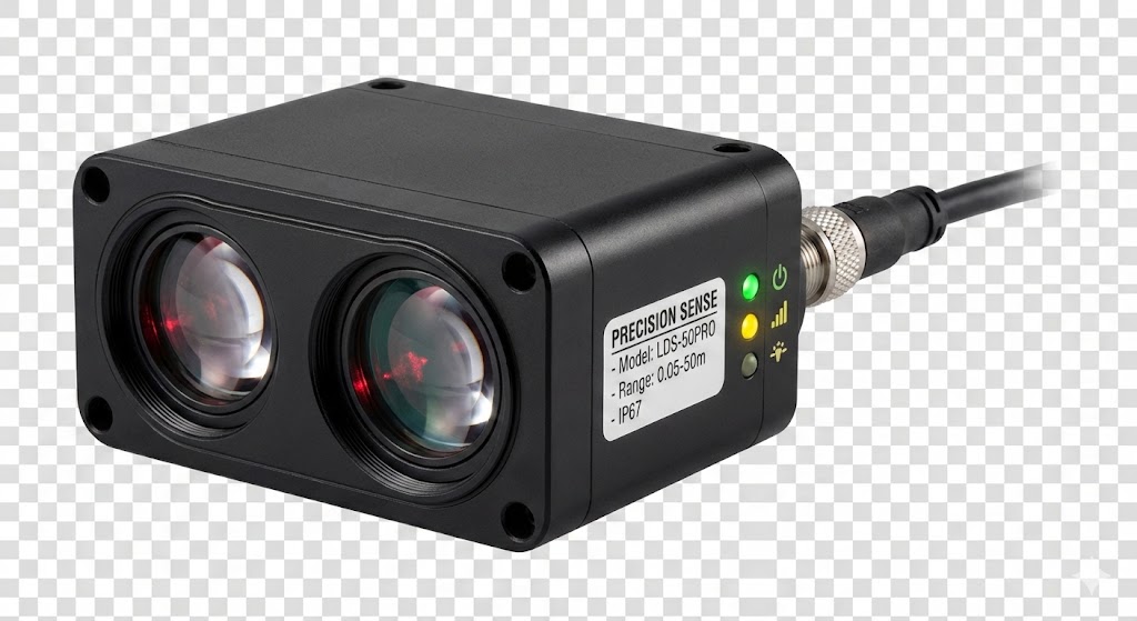
Selecting the appropriate SMT laser displacement sensor requires careful consideration of several technical specifications. Measurement range and stand-off distance define the working envelope. A sensor with a smaller range typically offers higher resolution. Resolution and repeatability are paramount; resolution is the smallest detectable change, while repeatability indicates measurement consistency. For SPI, sub-micron resolution is often necessary. Spot size is crucial—a smaller laser spot allows for measuring finer features like narrow solder paste deposits or small component leads. Sampling speed must match the production line's throughput; high-speed lines demand sensors with kHz-level sampling rates to inspect every board without becoming a bottleneck. Environmental robustness is non-negotiable. Sensors must withstand factory-floor vibrations, temperature fluctuations, and potential contamination from flux or dust. Models with IP ratings and robust housings are preferred.
Integration is another key factor. Modern sensors offer digital interfaces (Ethernet/IP, PROFINET, RS-232) for seamless communication with PLCs and factory host systems. Built-in software tools for profile analysis, pass/fail judgment, and data logging are essential for inline process control. Finally, the choice between a confocal chromatic sensor (offering very high precision on reflective surfaces) and a standard laser triangulation sensor (excellent for most SMT materials) depends on the specific surface characteristics being measured.
In conclusion, SMT laser displacement sensors are the eyes of the automated assembly line, providing the precise, reliable, and fast 3D measurement data that modern electronics manufacturing demands. From ensuring perfect solder paste deposition to verifying component integrity, their role is foundational to achieving high first-pass yields and ultimate product reliability. Understanding their technology and selection criteria empowers engineers to build more capable, efficient, and quality-focused production systems.