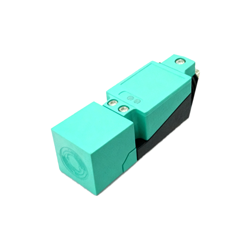
Proximity sensors are indispensable components in modern industrial automation, offering non-contact detection of objects with high precision and reliability. Understanding the internal structure and schematic diagram of a small proximity sensor is crucial for engineers to optimize system design, troubleshoot issues, and ensure seamless integration into various applications. This article delves into the detailed schematic representation and structural composition of a typical inductive proximity sensor, widely used in manufacturing, robotics, and automotive industries.
A standard inductive proximity sensor comprises several key components, each playing a vital role in its operation. The core element is the oscillator circuit, which generates a high-frequency electromagnetic field from the sensing face. This field is typically produced by a coil wound around a ferrite core, connected to an oscillator IC. When a metallic object enters this field, eddy currents are induced on the object's surface, causing a change in the oscillation amplitude. This change is detected by an amplitude detection circuit, which then triggers a signal conditioning unit.
The signal conditioning unit processes the detected change and forwards it to a switching circuit, often involving a transistor or solid-state relay. This circuit controls the output state, switching it ON or OFF based on the presence or absence of the target. The output is usually configured as either NPN (sinking) or PNP (sourcing), with options for normally open (NO) or normally closed (NC) contacts. Power supply connections, typically ranging from 10-30V DC, are integrated into the schematic, along with protection diodes to guard against reverse polarity and voltage spikes.
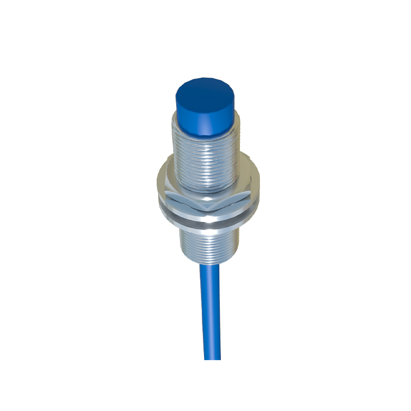
Encapsulating these electronic components is a robust housing made of materials like nickel-plated brass or stainless steel, ensuring durability in harsh environments. The sensing face is protected by a front cap, often constructed from PTFE or similar wear-resistant plastics. Internal shielding minimizes electromagnetic interference (EMI), while LED indicators provide visual status feedback. Wiring diagrams accompanying the schematic illustrate proper connection to PLCs, controllers, or other devices, highlighting terminal assignments for power, ground, and output signals.
Engineers must consider factors such as sensing distance, response time, and environmental conditions when interpreting schematics. For instance, temperature variations can affect oscillator stability, necessitating compensation circuits in high-precision models. Additionally, modern sensors may include diagnostic features like short-circuit protection or IO-Link communication interfaces, reflected in more complex schematic layouts. By mastering these diagrams, professionals can enhance system reliability, reduce downtime, and innovate in automation solutions.
In summary, the schematic diagram of a small proximity sensor reveals a sophisticated interplay of electromagnetic principles and electronic circuitry. From oscillator to output stage, each component is meticulously designed to deliver accurate, non-contact detection. As Industry 4.0 advances, familiarity with these structures empowers engineers to leverage sensor technology for smarter, more efficient industrial operations.