In the rapidly evolving landscape of sensor technology, the demand for miniaturization, reliability, and high-performance packaging has never been greater. As a seasoned electrical engineer specializing in advanced manufacturing, I have observed laser welding emerge as a critical, transformative process for fabricating sensor samples and prototypes. This article delves into the technical intricacies, advantages, and application-specific considerations of employing laser welding in sensor development.
Fundamentally, laser welding is a fusion welding process that utilizes a highly focused laser beam as a concentrated heat source to join materials. For sensor assemblies, which often involve delicate components, dissimilar metals, and hermetic seals, this method offers unparalleled precision. The laser's energy can be precisely controlled in terms of power density, pulse duration, and spot size—often down to micrometer scales. This allows for extremely localized heating, minimizing the Heat-Affected Zone (HAZ). A minimal HAZ is paramount for sensor samples, as excessive thermal input can degrade sensitive internal elements like MEMS structures, piezoelectric crystals, or semiconductor dies, ultimately compromising calibration and long-term stability.
The process typically involves either conduction welding for shallower, cosmetic seams or keyhole welding for deeper penetration. For sensor housings requiring hermeticity—such as those for pressure transducers, inertial measurement units (IMUs), or medical sensors—keyhole welding is often employed to create a deep, narrow weld seam that ensures a leak-tight seal. The choice of laser source is also critical. Fiber lasers and pulsed Nd:YAG lasers are predominant in this domain. Fiber lasers, with their high beam quality and efficiency, are excellent for high-speed, precise welding of reflective metals like aluminum and copper alloys commonly used in sensor casings. Pulsed lasers provide excellent control over heat input, making them ideal for welding thin foils, tiny pins, or dissimilar material joints without causing thermal distortion.
Material compatibility is a central consideration. Sensor samples frequently involve joining dissimilar metals, such as Kovar to glass for feedthroughs or stainless steel to aluminum for lightweight housings. Laser welding's rapid cooling rate can help manage the formation of brittle intermetallic compounds in such joints. Furthermore, the process is often performed in an inert gas atmosphere (e.g., argon or nitrogen) to prevent oxidation, ensuring a clean, strong weld bead critical for both mechanical integrity and corrosion resistance.
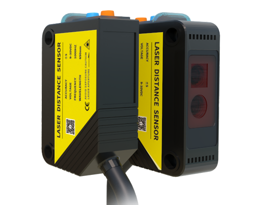
From a prototyping and sample development perspective, laser welding offers significant flexibility. Computer Numerical Control (CNC) and galvanometer scanner systems enable complex, non-contact weld paths to be programmed with high repeatability. This is invaluable for creating small batches of sensor samples for functional testing and validation. Engineers can quickly iterate on package designs, test different weld seam geometries, and evaluate hermeticity without the need for expensive hard tooling required by traditional welding methods. The ability to weld in difficult-to-access areas is another key benefit, allowing for innovative, compact sensor designs that were previously unmanufacturable.
However, the process is not without its challenges. Joint fit-up must be exceptionally precise, as the laser beam has little tolerance for gaps. Surface preparation is crucial; contaminants can lead to porosity and weak welds. Furthermore, the high capital cost of industrial laser systems and the need for specialized operator expertise are barriers, though these are often justified by the superior quality and yield in high-value sensor applications.
In conclusion, laser welding represents a cornerstone technology for the development of next-generation sensor samples. Its precision, low thermal impact, and design flexibility directly address the core requirements of modern sensor packaging: integrity, miniaturization, and reliability. As sensor applications expand into more demanding environments—from automotive powertrains to implantable medical devices—the role of laser welding in translating prototype designs into viable, high-performance products will only become more pronounced. For any engineering team embarking on sensor development, a deep understanding of this process is not just an advantage; it is a necessity for achieving technical and commercial success.