Proximity sensors are fundamental components in modern industrial automation, robotics, and countless electronic devices. Their primary function is to detect the presence or absence of an object within a specified range without any physical contact. To truly grasp how they operate, one must delve into their schematic diagrams, which serve as the blueprint for their functionality. This article will dissect the typical schematic representation of a common type—the inductive proximity sensor—explaining each component's role and the underlying operational principles.
At its core, the schematic diagram of an inductive proximity sensor reveals a circuit centered around an oscillator, a detection circuit, and an output stage. The process begins with the oscillator coil, which is part of the sensor's sensing face. In the schematic, this coil (L1) is connected to an oscillator circuit, often built around a transistor or an integrated oscillator chip. This circuit generates a high-frequency electromagnetic field that radiates from the sensor's active surface. The schematic clearly shows the oscillator's components: resistors (R1, R2) for biasing, a capacitor (C1) for tuning the frequency, and the coil itself forming the inductive element of the LC tank circuit.
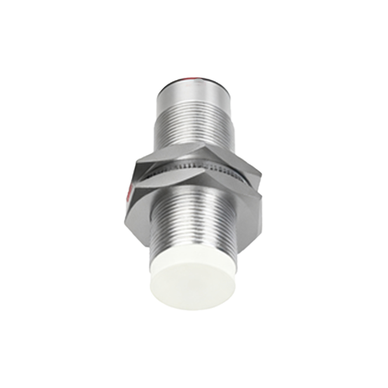
When no metallic target is present within the sensing range, the oscillator runs freely at its designed frequency, maintaining a steady amplitude. This state is represented in the schematic by a stable signal path from the oscillator to the next stage: the detector or trigger circuit. This circuit, often comprising a comparator or a specific detection IC, continuously monitors the oscillator's amplitude.
The fundamental principle of detection is depicted in the schematic's signal flow. When a metallic object enters the oscillating electromagnetic field, eddy currents are induced on the surface of the target. These currents draw energy from the oscillator, as shown symbolically by a load effect on coil L1 in the diagram. This energy loss causes a measurable decrease in the amplitude of the oscillator's oscillation. The detection circuit is precisely designed to sense this amplitude drop. In the schematic, the comparator (IC1) compares the damped oscillator signal against a fixed reference voltage (Vref). Once the amplitude falls below this threshold, the comparator's output state changes.
This change in the detection circuit's output triggers the final stage: the output driver. The schematic illustrates this section, which is responsible for switching the sensor's output signal. For a standard three-wire DC sensor, the output is typically an NPN or PNP transistor. In an NPN configuration (sourcing output), the transistor's base is driven by the detection circuit. When activated, it allows current to flow from the load, through the output wire (usually black), into the collector, and out through the emitter to the common (negative) terminal. The schematic includes protective components like a freewheeling diode (D1) across the output transistor to suppress voltage spikes from inductive loads, and often a status LED (LED1) with a current-limiting resistor (R3) to provide visual indication of the output state.
Power supply connections are clearly marked: V+ (brown wire) for positive supply and V- (blue wire) for the common/ground. The schematic also shows internal voltage regulation, often via a Zener diode or regulator IC, to ensure stable operation for the oscillator and logic circuits despite variations in the supply voltage.
Understanding this schematic is crucial for troubleshooting, integration, and selection. It explains why inductive sensors only detect metals, as non-conductive materials do not generate significant eddy currents. It also clarifies key specifications like sensing distance, which is influenced by the oscillator's power and coil design, and switching frequency, determined by the speed of the oscillator, detector, and output stages.
In summary, the schematic diagram of a proximity sensor is not merely a collection of symbols but a detailed map of its non-contact detection journey. From the generation of an electromagnetic field to the sensing of its disturbance, and finally to the clean switching of an output signal, each component plays a vital role. By interpreting this diagram, engineers and technicians can fully appreciate the elegant electronic principles that enable these versatile devices to form the invisible touchpoints of automated systems.