In the realm of industrial automation and control systems, proximity sensors are indispensable components for non-contact object detection. Among these, anti-interference proximity sensors stand out for their reliability in electrically noisy environments. A thorough understanding of their structural diagram is crucial for engineers to ensure optimal selection, installation, and troubleshooting. This article delves into the key components and operational principles illustrated in a typical structural diagram of an anti-interference proximity sensor.
The core of the sensor is the sensing element, often a coil wound around a ferrite core, which forms part of an oscillator circuit. This oscillator generates a high-frequency electromagnetic field at the active face of the sensor. In inductive-type sensors, when a metallic target enters this field, eddy currents are induced, causing a change in the oscillation amplitude. This change is detected by the subsequent circuitry. The structural diagram clearly demarcates this oscillator section, showing the coil's connection to the oscillation circuit components.
The defining feature of an anti-interference model is its sophisticated signal processing and conditioning block. Following the oscillator, the diagram shows an amplitude detection or demodulation stage. This stage converts the oscillation amplitude change into a DC voltage signal. However, the critical components for noise immunity are the filters and the specialized evaluation circuitry. The structural diagram typically highlights integrated band-pass filters that allow only the specific frequency band of the oscillator's signal to pass, effectively rejecting lower-frequency power line noise and higher-frequency switching transients from motors or inverters.
Furthermore, the diagram illustrates the shielding and housing design. A robust metal casing, often made of stainless steel like V2A or V4A, surrounds the internal electronics. This casing acts as both a mechanical shield and a Faraday cage, preventing external electromagnetic fields from penetrating and interfering with the sensitive oscillator circuit. The diagram might show this as a grounded, continuous enclosure. Special attention is given to the front face, where a non-metallic sensing surface (e.g., PTFE or ceramic) allows the field to emanate while protecting the coil.
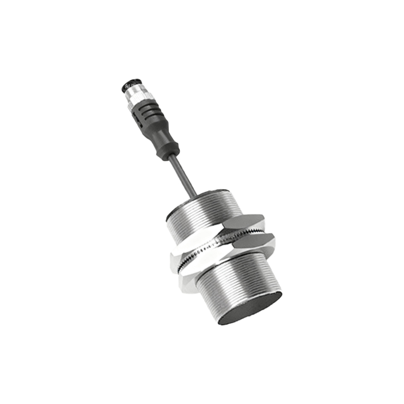
The output stage is another key area depicted. After signal conditioning, the processed signal triggers a solid-state switch. Common outputs include NPN, PNP, or push-pull configurations. The structural diagram details the output transistor and the protective components such as flyback diodes for DC models or surge suppressors for overvoltage protection. These elements safeguard the sensor from voltage spikes commonly found in industrial settings, which are a form of conducted interference.
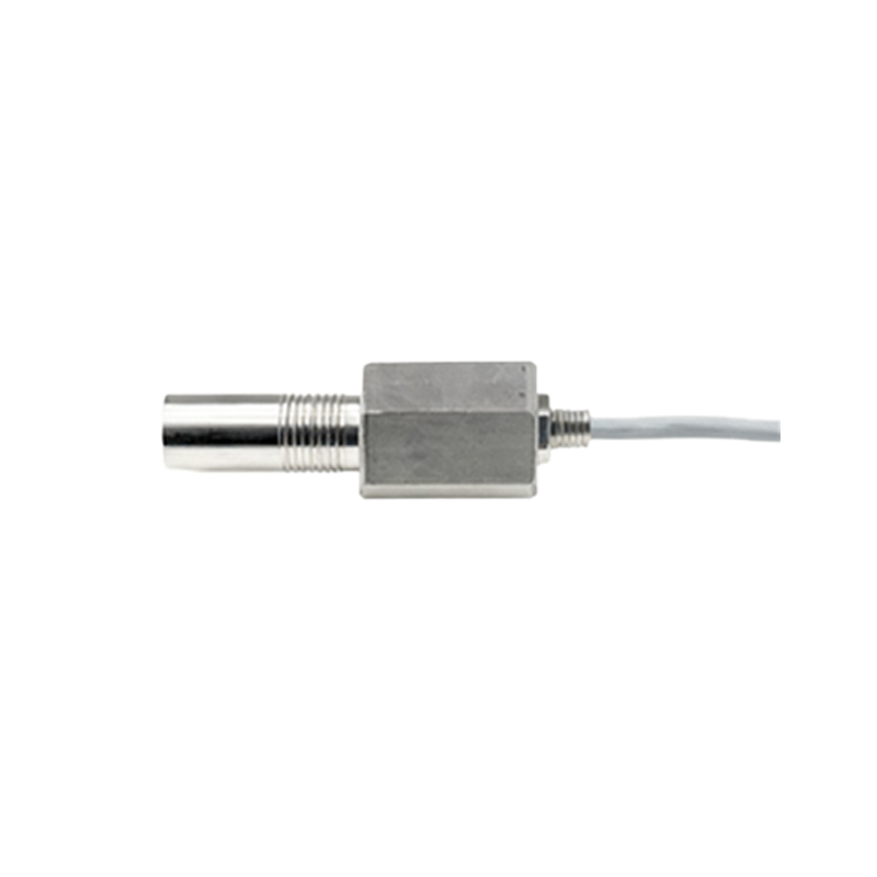
Wiring and connection points are explicitly shown. A standard three-wire or two-wire configuration is illustrated, with clear markings for supply voltage (V+), ground (0V), and the output signal line. The diagram emphasizes the importance of shielded cables, with the shield connected to the ground at the controller side to drain away noise currents. Some advanced diagrams for analog sensors also show the signal characteristic curve relative to the sensing distance.
Understanding the interplay between these components on the diagram explains the sensor's operation. The oscillator generates the field; the target causes a change; the demodulator converts it; filters strip away noise; and the evaluation circuit makes a precise switching decision, which is then communicated via the protected output stage. The physical structure, with its shielding and specialized face material, ensures this process remains unaffected by ambient conditions.
In conclusion, the structural diagram of an anti-interference proximity sensor is a blueprint of its robustness. It maps the journey from electromagnetic field generation to a clean, reliable output signal, highlighting every design element—from internal filters and shielded housings to output protection—that collectively combat electrical interference. For engineers, mastering this diagram is not merely academic; it is essential for deploying sensors that guarantee precision and longevity in the challenging electromagnetic landscape of modern factories.