In the realm of modern electronics, from smartphones and tablets to industrial automation and automotive systems, proximity sensors play a pivotal role in enabling intuitive, touch-free interactions and critical safety functions. However, the performance of these sophisticated components is not solely determined by their inherent specifications. The physical layout and integration of the sensor into the final product design are equally, if not more, crucial. A poorly designed sensor layout can lead to erratic behavior, reduced sensing range, false triggers, and ultimately, a degraded user experience or system failure. This article delves into the fundamental principles and best practices for effective proximity sensor layout design, ensuring reliable and consistent operation.
The primary objective of layout design is to maximize the signal-to-noise ratio (SNR) for the sensor. The "signal" is the intended reflection from a target object, while "noise" encompasses all unwanted electrical and optical interference. The layout must be optimized to enhance the former and mitigate the latter. The first and most critical step is a thorough review of the sensor manufacturer's datasheet and application notes. These documents provide essential guidelines specific to the component, including recommended keep-out areas, aperture design, and material considerations.
One of the most significant challenges is managing infrared (IR) interference, common in IR-based proximity sensors. The sensor's IR emitter and receiver must be optically isolated to prevent internal crosstalk, where emitted light directly leaks into the receiver without an external target. This is achieved through careful mechanical design. Using a barrier wall—a physical septum made of non-reflective, opaque material between the emitter and receiver—is a standard and highly effective method. This wall should extend from the sensor package right up to the inner surface of the product's external cover or lens.
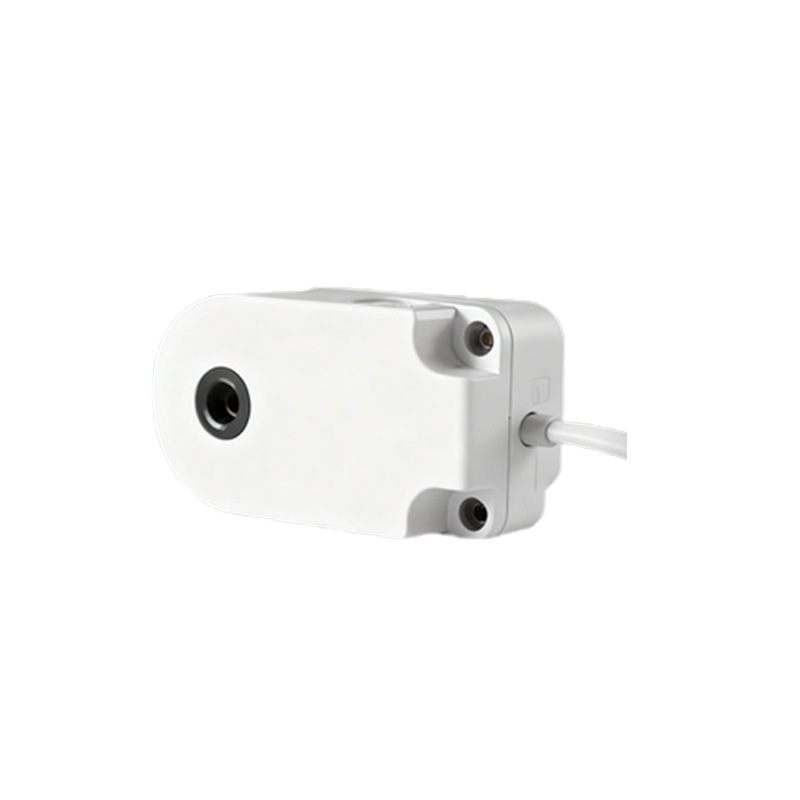
The design of the aperture—the opening in the product's outer casing through which the IR light passes—is paramount. The aperture must be precisely aligned with the sensor's optical axis. Its size and shape should be optimized to limit the field of view (FOV) of both the emitter and receiver, reducing susceptibility to ambient light and unwanted reflections from the product's own bezel or housing. A smaller, tailored aperture improves directionality but must be balanced against potential signal reduction. The aperture edges should be clean and sharp to minimize internal scattering. Often, the use of a separate infrared-transmissive window or lens made of materials like polycarbonate with specific IR coatings is necessary. This window must be seamlessly integrated to avoid air gaps or cosmetic defects that can cause unpredictable reflections.
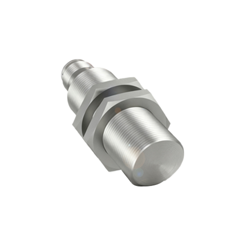
Material selection for the surrounding area is another vital factor. The interior surfaces near the sensor, especially the area directly behind the aperture, should be coated with a matte, non-reflective black finish. This absorbs stray IR light instead of reflecting it back to the receiver. Materials like textured black plastic or specialized IR-absorbing paints are commonly used. Conversely, highly reflective materials like shiny metal or white plastic must be avoided in the sensor's optical path.
Electrical layout on the printed circuit board (PCB) is just as important as the mechanical design. The sensor should be placed away from noisy components such as switching regulators, high-speed digital lines, or RF antennas. Power supply lines to the sensor must be clean and stable, often requiring dedicated local filtering with capacitors as specified in the datasheet. The sensor's signal traces should be kept short and, if possible, routed on an inner layer shielded by ground planes to minimize electromagnetic interference (EMI). Proper grounding techniques are essential to create a stable reference and shunt noise away from the sensitive analog front-end of the receiver.
Environmental factors must also be considered during the layout phase. For products used outdoors or in variable lighting, protection from sunlight and other strong ambient light sources is critical. The use of optical filters that match the sensor's IR wavelength can help reject out-of-band light. Additionally, the design must account for potential contamination from dust, moisture, or fingerprints on the external window, which can attenuate the signal. Some designs incorporate hydrophobic coatings or recessed apertures to mitigate these issues.
Finally, rigorous testing throughout the development cycle is non-negotiable. Layout efficacy should be validated under a wide range of real-world conditions: different target materials (skin, glass, plastic), various ambient lighting levels (darkness to direct sunlight), and extreme temperatures. Testing should also include scenarios that could cause false triggers, such as placing the device on a reflective surface. Data from this testing feeds back into iterative refinements of the mechanical and electrical layout.
In conclusion, a successful proximity sensor integration is a multidisciplinary exercise in optical, mechanical, and electrical engineering. There is no universal template; each product presents unique constraints. By adhering to core principles of optical isolation, aperture control, material management, and electrical cleanliness, engineers can design robust layouts that unlock the full, reliable potential of proximity sensing technology, creating products that are both intelligent and dependable.