Laser CMOS sensors represent a sophisticated fusion of optical triangulation principles and advanced semiconductor imaging technology, forming a cornerstone of modern industrial automation, precision metrology, and quality control. At its core, the operational principle hinges on the precise measurement of distance or displacement by analyzing the position of a laser spot projected onto a target surface. A laser diode emits a focused, coherent beam of light—typically in the visible red or infrared spectrum—which strikes the object under inspection. The diffusely reflected light from this illuminated spot is then collected by a lens and focused onto a specialized CMOS (Complementary Metal-Oxide-Semiconductor) linear or area image sensor.
The CMOS sensor is the critical electronic component that converts the optical signal into quantifiable digital data. Unlike its CCD (Charge-Coupled Device) predecessor, a CMOS sensor integrates amplification and digitization circuitry at each pixel site, offering advantages in speed, power consumption, and system integration. In a standard laser triangulation setup, the sensor, laser emitter, and target form a precise geometric triangle. Any change in the target's distance (Z-axis) causes the reflected laser spot to shift its position laterally (X-axis) across the active surface of the CMOS array. This displacement is not random but follows a strict trigonometric relationship defined by the fixed baseline distance between the laser source and the sensor's receiving lens.
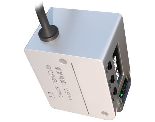
The sensor's pixel array captures the spot's image at an extremely high frame rate. On-chip processing algorithms, often supported by a dedicated microcontroller or FPGA, then perform a centroid calculation to determine the spot's exact center with sub-pixel accuracy. This calculation is crucial as it allows the system to resolve movements much smaller than the physical size of an individual pixel. The computed centroid position is directly correlated to the target distance via a pre-calibrated lookup table or a mathematical model. This entire process, from laser emission to distance output, occurs in microseconds, enabling real-time, non-contact measurement.
Key performance parameters are deeply intertwined with the CMOS sensor's characteristics. Resolution is a function of optical magnification, sensor pixel pitch, and the signal-to-noise ratio of the detected spot. Measurement range is determined by the sensor's length (for linear sensors) or dimensions (for area sensors) and the triangulation angle; a narrower angle offers a longer range but potentially lower resolution, and vice-versa. The laser's wavelength and power, along with the target surface's optical properties (color, roughness, material), significantly influence signal strength. Highly reflective or specular surfaces can saturate the sensor, while dark, absorbent, or transparent materials may weaken the signal. Advanced sensors employ techniques like adaptive laser power control, multiple integration times, or specialized optical filters to handle such challenging surfaces.
Furthermore, the programmability of modern CMOS sensors enables sophisticated functionalities beyond simple point measurement. By modulating the laser into a line or a structured pattern and using a 2D CMOS matrix, these systems can perform profile scanning and 3D contour mapping. Each point along the laser line provides a height value, generating a detailed cross-sectional profile of an object as it moves relative to the sensor or as the laser line is swept across it.
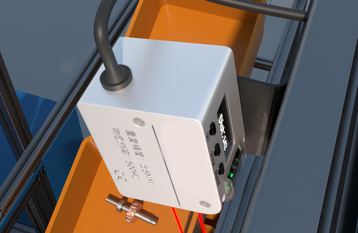
In industrial environments, robustness is paramount. Laser CMOS sensors are engineered to withstand vibration, ambient light interference, temperature fluctuations, and electromagnetic noise. Housing is typically ruggedized to IP67 standards or higher. The digital nature of CMOS technology facilitates easy interfacing with industrial networks like Ethernet/IP, PROFINET, or EtherCAT, streamlining integration into larger control systems.
Applications are vast and critical. In automotive manufacturing, they measure body panel gaps and flushness with micron-level precision. In electronics, they verify component coplanarity and solder paste height. In logistics, they measure package dimensions for volumetric sorting. In robotics, they provide essential feedback for bin-picking and guided assembly. The non-contact nature prevents part damage or deformation, a significant advantage over tactile probes.
The ongoing evolution of CMOS fabrication technology continues to push the boundaries of laser sensor performance. Smaller pixel sizes increase spatial resolution, while improved global shutter designs eliminate motion blur for high-speed applications. Enhanced on-chip processing capabilities allow for edge computing, where data filtering and preliminary analysis occur within the sensor itself, reducing latency and load on central controllers. Integration with AI algorithms for anomaly detection and classification is an emerging frontier, transforming the sensor from a mere data collector into an intelligent perception node.

In conclusion, the laser CMOS sensor is a paradigm of precision optoelectronics. Its principle, rooted in simple triangulation, is empowered by the versatility and computational power of CMOS imaging technology. It delivers fast, accurate, and reliable non-contact measurements that are indispensable for enhancing productivity, ensuring quality, and enabling advanced automation across countless industries. As CMOS technology advances, so too will the capabilities and applications of these vital sensing tools.