Area laser sensors represent a significant advancement in non-contact measurement and detection technology. Unlike traditional point or line lasers, these devices project a two-dimensional laser pattern—often a fan, grid, or structured light shape—onto a target surface. By analyzing the deformation, displacement, or profile of this projected pattern using a complementary imaging sensor (like a CMOS or CCD camera), the system can extract precise three-dimensional information about the object. The core principle involves triangulation; the known baseline distance between the laser projector and the camera, combined with the observed distortion of the laser pattern, allows for accurate calculation of depth and surface contours.
The operational methodology is both elegant and powerful. A laser diode emits a coherent light pattern. When this pattern strikes an object, its shape changes based on the object's surface geometry. A lens system focuses this altered pattern onto the image sensor. Sophisticated onboard processors then execute algorithms to compare the received image with a reference pattern (often calibrated on a known flat plane). This comparison yields a dense point cloud or height map, providing detailed topographic data. Key performance parameters include measurement range, resolution, scanning frequency, and field of view. Modern sensors achieve remarkably high speeds, capable of processing thousands of profiles per second, making them suitable for dynamic inspection lines.
The advantages of area laser sensors are manifold. They deliver high-speed, high-resolution 3D data without physical contact, preserving delicate surfaces. Their ability to capture an entire area in a single shot eliminates the need for scanning motions required by point sensors, drastically increasing throughput. They are largely immune to ambient light interference when equipped with optical filters tuned to the laser's wavelength, ensuring reliability in industrial environments. Furthermore, they provide rich data sets that enable complex inspections beyond simple distance checking.
Applications span numerous industries, driving automation and quality control. In automotive manufacturing, they are deployed for gap and flush measurement between body panels, weld seam inspection, and robotic guidance for assembly. The electronics industry relies on them for solder paste inspection (SPI), component coplanarity checks, and PCB warpage measurement. In logistics and warehousing, they facilitate volumetric dimensioning of packages for optimal storage and shipping cost calculation. Additional uses include reverse engineering, cultural heritage preservation through 3D scanning, and even medical applications like custom orthotic design.
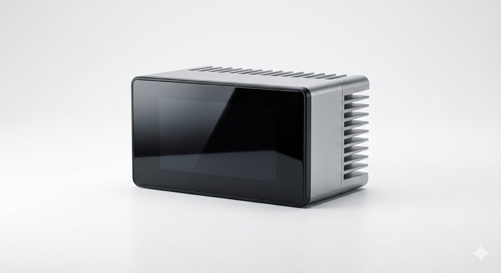
Selecting the appropriate area laser sensor requires careful consideration of the specific task. Engineers must evaluate the required measurement range, the necessary spatial and height resolution, the object's surface properties (highly reflective or absorbent surfaces pose challenges), and the environmental conditions such as vibration or temperature extremes. Integration aspects are equally crucial, involving compatibility with factory networks (Ethernet/IP, PROFINET), software development kits (SDKs) for custom application development, and mechanical mounting for stable operation.
Looking ahead, the evolution of area laser sensor technology points toward even greater miniaturization, enhanced processing power enabling edge computing and AI-based real-time defect classification, and reduction in cost. Integration with other sensing modalities, like RGB cameras for combined 2D and 3D data fusion, is becoming more common. These trends will further solidify their role as indispensable tools in the fourth industrial revolution, enabling smarter, more adaptive, and highly precise automated systems across the global manufacturing and research landscape.