Laser distance sensors have become indispensable tools across industries, from construction and surveying to robotics and industrial automation. Their ability to provide rapid, precise, and non-contact measurements has revolutionized numerous processes. But what exactly lies within the sleek housing of these devices? This technical teardown aims to dissect a typical time-of-flight (ToF) based laser distance sensor, exploring its core components, operational principles, and the engineering considerations behind its design.
Our subject is a common industrial-grade module with a stated measurement range of 0.05 to 40 meters and an accuracy of ±1.5 mm. The external casing, typically made of anodized aluminum, provides durability, electromagnetic shielding, and acts as a heat sink for internal components. Removing the several small screws reveals the internal architecture. Immediately apparent is the clear segregation of optical and electronic assemblies, a critical design practice to minimize interference.
The optical front-end is centered around the laser diode, usually a Class 2 visible red laser or a Class 1 infrared laser for eye safety. It is precisely mounted in a collimating lens holder. This lens assembly is crucial for producing a tight, low-divergence beam, ensuring the emitted light travels as a coherent spot to the target. Adjacent to the emitter is the receiving optics. This consists of a collection lens, often an aspherical lens to reduce aberrations, which focuses the reflected laser light onto a highly sensitive photodetector. A critical filter is placed in front of this detector—an optical bandpass filter matched precisely to the laser's wavelength. This filter dramatically attenuates ambient light (from sunlight or room lighting), allowing the sensor to function reliably in various lighting conditions.
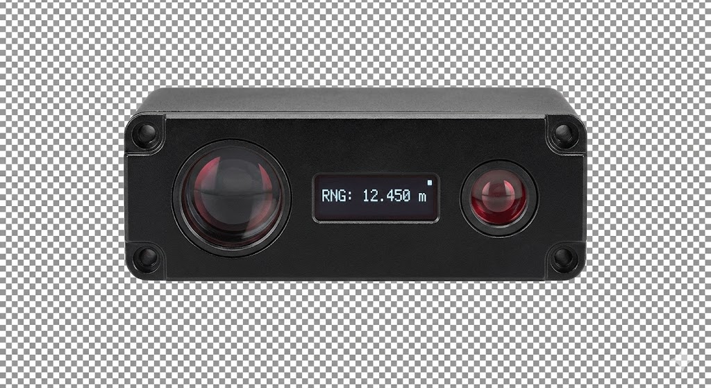
The heart of the electronic system is the dedicated ToF sensor IC or a high-speed microcontroller with specialized peripherals. This chip is responsible for the precise timing that defines the time-of-flight principle. It generates a modulated signal to drive the laser diode. The laser beam is not emitted as a simple pulse but as a high-frequency modulated wave, often in the MHz range. The same light, after reflecting off the target, is detected by the photodetector (typically an avalanche photodiode or PIN photodiode for its fast response). The received signal is extremely weak and is immediately amplified by a low-noise transimpedance amplifier (TIA).
The core measurement occurs by comparing the phase shift between the emitted modulated signal and the received signal. The ToF processor performs this phase detection with remarkable precision. Since the speed of light is a known constant, the measured phase shift directly correlates to the time the light spent traveling to the target and back. This time, multiplied by the speed of light and divided by two (for the round trip), yields the distance. This phase-shift method is favored over simple pulse timing for short to medium ranges due to its superior accuracy and noise immunity.
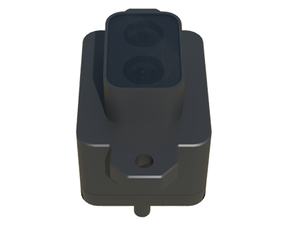
Surrounding the main processor are supporting circuits: a stable voltage regulator ensuring clean power, memory chips for storing calibration data, and communication interfaces like UART (TTL or RS-232), I2C, or analog output drivers. Calibration is paramount. Each sensor is factory-calibrated against known distances, and compensation algorithms within the firmware account for minor component variances and environmental factors like temperature, which can affect laser output and electronic timing.
Several engineering challenges are evident in the layout. The high-speed signal path from the photodetector to the amplifier is kept extremely short to minimize parasitic capacitance and noise pickup. The laser driver circuit is isolated to prevent electrical noise from disrupting the sensitive receiving channel. Thermal management is also considered, with thermal pads often connecting the laser diode and main IC to the metal housing.
In conclusion, a laser distance sensor is a sophisticated fusion of precision optics, analog signal conditioning, and high-speed digital processing. The teardown reveals a design optimized for signal integrity, noise rejection, and environmental robustness. Understanding this internal composition not only demystifies its operation but also highlights the careful engineering required to achieve millimeter-level accuracy in a compact, reliable package suitable for demanding industrial applications. Future trends point towards further miniaturization, the integration of multi-sensor data fusion, and the use of VCSEL (Vertical-Cavity Surface-Emitting Laser) arrays for more advanced scanning and profiling capabilities.